8
Notes:
1. The LED is ON when V
I
is low and OFF when V
I
is high.
2. t
PHL
propagation delay is measured from the 50% level on the falling edge of the V
I
signal to the 50% level of the falling edge of the V
O
signal.
t
PLH
propagation delay is measured from the 50% level on the rising edge of the V
I
signal to the 50% level of the rising edge of the V
O
signal.
3. Mimimum Pulse Width is the shortest pulse width at which 10% maximum, Pulse Width Distortion can be guaran teed. Maximum Data Rate is
the inverse of Minimum Pulse Width. Operating the HCPL-x710 at data rates above 12.5 MBd is possible provided PWD and data dependent
jitter increases and relaxed noise margins are tolerable within the application. For instance, if the maximum allowable variation of bit width is
30%, the maximum data rate becomes 37.5 MBd. Note: HCPL-x710 performances above 12.5 MBd are not guaranteed by Avago.
4. PWD is dened as |t
PHL
- t
PLH
|. %PWD (percent pulse width distortion) is equal to the PWD divided by pulse width.
5. t
PSK
is equal to the magnitude of the worst case dierence in t
PHL
and/or t
PLH
that will be seen between units at any given temperature within
the recommended operating conditions.
6. CM
H
is the maximum common mode voltage slew rate that can be sustained while maintaining V
O
> 0.8 V
DD2
. CM
L
is the maximum common
mode voltage slew rate that can be sustained while maintaining V
O
< 0.8 V. The common mode voltage slew rates apply to both rising and
falling common mode voltage edges.
7. Unloaded dynamic power dissipation is calculated as follows: C
PD
* V
DD2
* f + I
DD
* V
DD
, where f is switching frequency in MHz.
8. Device considered a two-terminal device: pins 1, 2, 3, and 4 shorted together and pins 5, 6, 7, and 8 shorted together.
9. In accordance with UL1577, each HCPL-0710 is proof tested by applying an insulation test voltage ≥4500 V
RMS
for 1 second (leakage detec-
tion current limit, I
I-O
≤5 µA). Each HCPL-7710 is proof tested by applying an insulation test voltage ≥ 4500 V
RMS
for 1 second (leakage detec-
tion current limit, I
I-O
≤ 5 µA).
10. The Input-Output Momentary With stand Voltage is a dielectric voltage rating that should not be interpreted as an input-output continuous
voltage rating. For the continuous voltage rating refer to your equipment level safety specication or Avago Application Note 1074 entitled
“Optocoupler Input-Output Endurance Voltage.”
11. C
I
is the capacitance measured at pin 2 (V
I
).
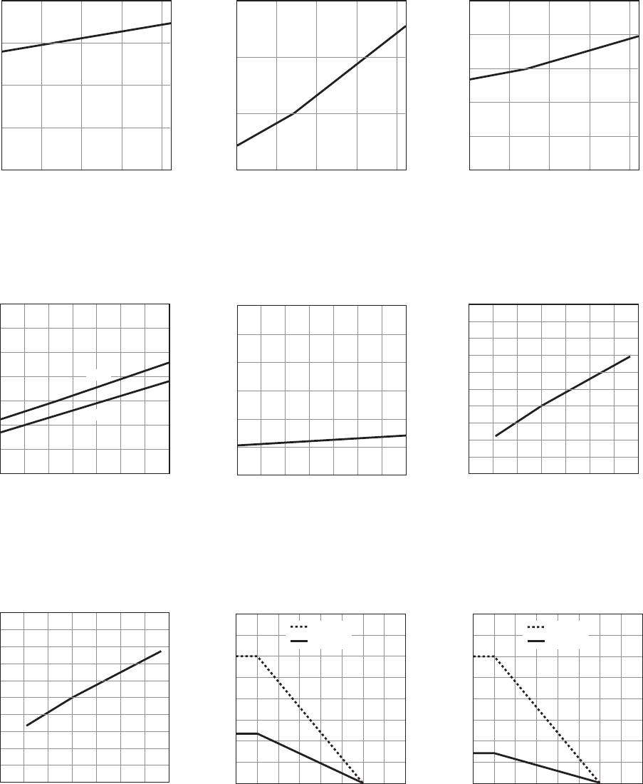
Figure 1. Typical output voltage vs. input
voltage
Figure 2. Typical input voltage switching
threshold vs. input supply voltage
Figure 3. Typical propagation delays vs. tem-
perature
Package Characteristics
Parameter Symbol Min. Typ. Max. Units Test Conditions
Input-Output Momentary
Withstand Voltage
[8, 9, 10]
0710 V
ISO
3750 Vrms RH = 50%,
t = 1 min.,
T
A
= 25 °C
7710 3750
Option 020 5000
Resistance
(Input-Output)
[8]
R
I-O
10
12
Ω
V
I-O
= 500 V
dc
Capacitance
(Input-Output)
[8]
C
I-O
0.6 pF f = 1 MHz
Input Capacitance
[11]
C
I
3.0
Input IC Junction-to-Case
Thermal Resistance
-7710 q
jci
145 °C/W Thermocouple
located at center
underside of package
-0710 160
Output IC Junction-to-Case
Thermal Resistance
-7710 q
jco
140
-0710 135
Package Power Dissipation P
PD
150 mW
V
O
(V)
0
0
V
I
(V)
5
4
1
41 2 3
5
3
2
0 °C
25 °C
85 °C
V
ITH
(V)
4.5
1.6
V
DD1
(V)
5.5
2.1
1.7
5.254.75 5
2.2
2.0
1.8
1.9
0 °C
25 °C
85 °C
T
PLH
, T
PHL
(ns)
0
15
T
A
(C)
80
27
17
6020 30
29
25
19
21
10 40 50 70
23
T
PLH
T
PHL