I
NTEGRATED
C
IRCUITS
D
IVISION
DS-IX4340-R05 www.ixysic.com 1
Features
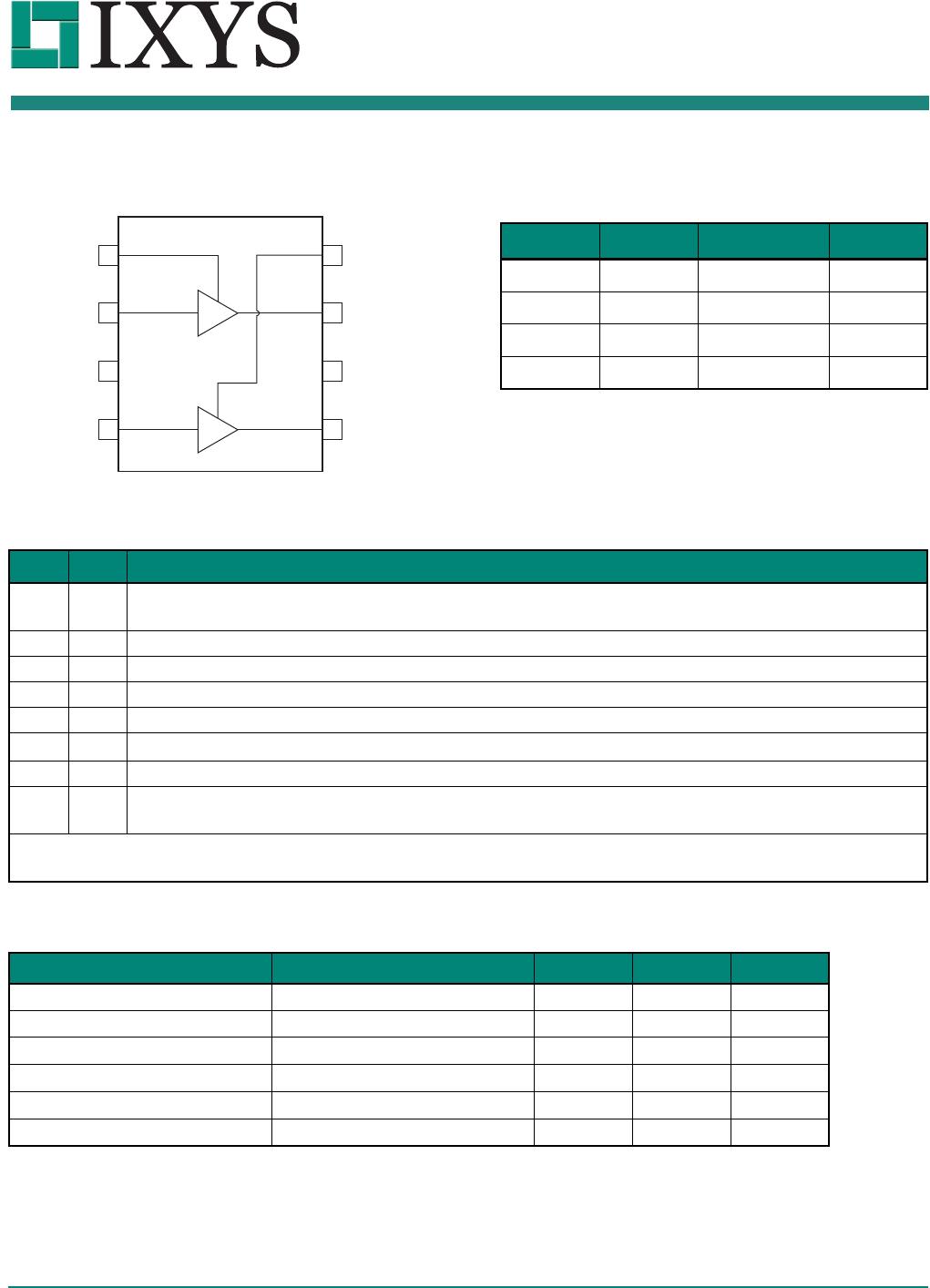
• Two Independent Drivers, Each Capable of Sourcing
and Sinking 5A
• CMOS and TTL Compatible Inputs
• Independent Enable for Each Driver
• 5V to 20V Supply Voltage Range
• -40°C to +125°C Extended Operating Temperature
Range
• ±4kV ESD Rating (Human Body Model)
• Thermally enhanced 8-pin SOIC and 8-pin MSOP
packages and standard 8-pin SOIC package
• Under Voltage Lockout Circuitry
• Fast Propagation Delays (16ns typical)
• Fast Rise and Fall Times (7ns typical)
Applications
• Switch-Mode Power Supplies
• DC-DC Converters
• Motor Controllers
• Power Inverters
Description
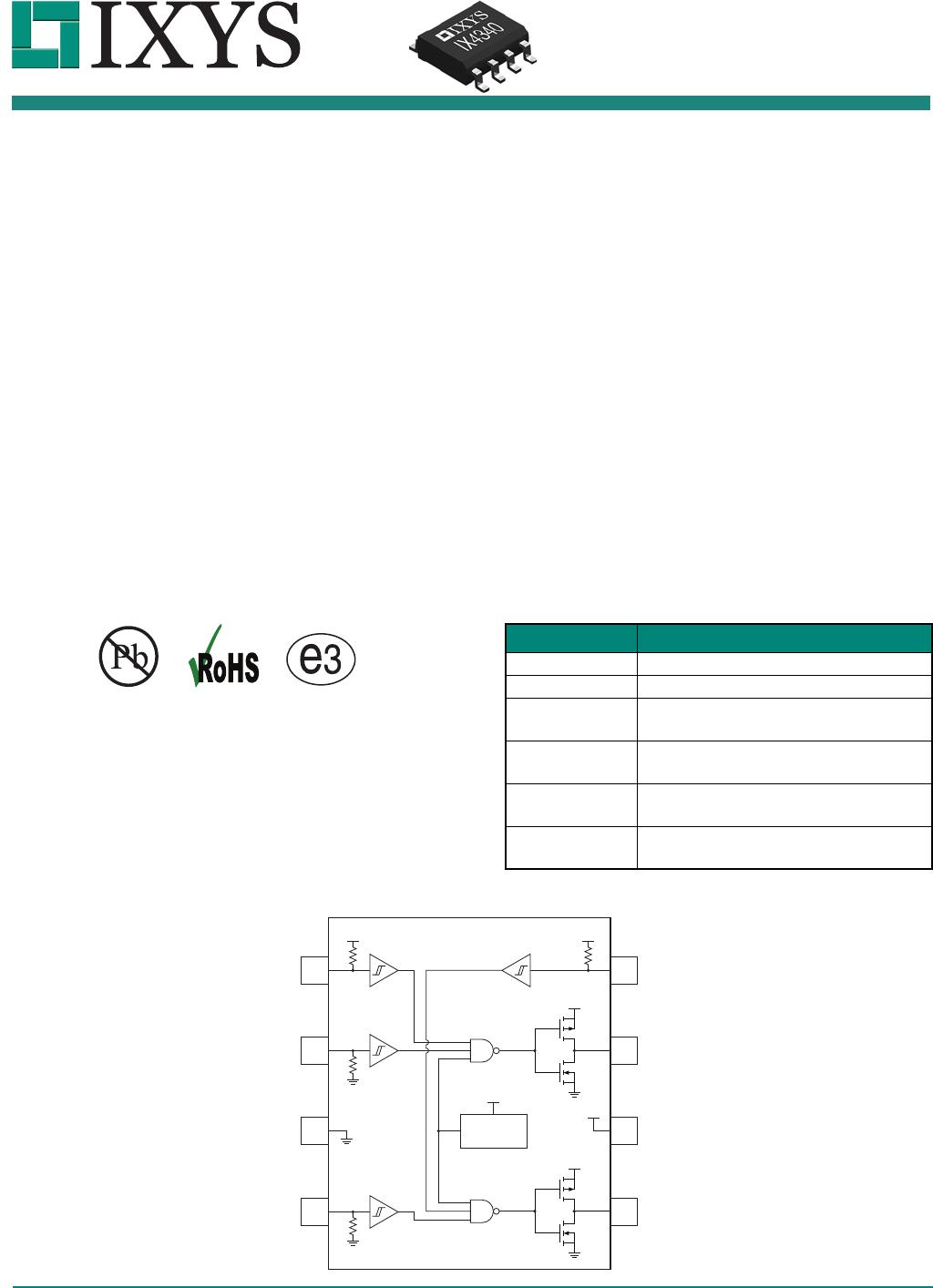
The IX4340 is a dual, high current, low side gate
driver. Each of the two outputs is capable of sourcing
and sinking 5A of peak current, and has a maximum
voltage rating of 20V. The two outputs can be
paralleled for higher current applications. Fast
propagation delay times (16ns typical) and fast rise
and fall times (7ns) make the IX4340 well suited for
high frequency applications.
The inputs are TTL and CMOS logic compatible, and
there is an independent Enable function for each
output. Under voltage lockout circuitry (UVLO)
prevents the high side source driver from conducting
until there is sufficient supply voltage. The outputs are
held low if the logic inputs are floating.
The IX4340 is available in standard 8-pin SOIC and
thermally enhanced 8-pin SOIC and MSOP packages.
Ordering Information
IX4340 Functional Block Diagram
Part Number Description
IX4340N 8-Pin SOIC (100/Tube)
IX4340NTR 8-Pin SOIC (4000/Reel)
IX4340NE
8-Pin SOIC w/ Exposed Thermal Pad
(100/Tube)
IX4340NETR
8-Pin SOIC w/ Exposed Thermal Pad
(4000/Reel)
IX4340UE
8-Pin MSOP w/ Exposed Thermal Pad
(100/Tube)
IX4340UETR
8-Pin MSOP w/ Exposed Thermal Pad
(5000/Reel)
V
CC
V
CC
V
CC
V
CC
V
CC
V
CC
UVLO
ENA
INA
GND
INB
ENB
OUTA
V
CC
OUTB
1
2
3
4
8
7
6
5
IX4340
5-Ampere, Dual Low-Side
MOSFET Driver