FEBRUARY 28, 2018 3 3-CHANNEL HIGH-PERFORMANCE TCXO/LVCMOS CLOCK BUFFER FAMILY
5PB12xx DATASHEET
Enable Function Truth Table
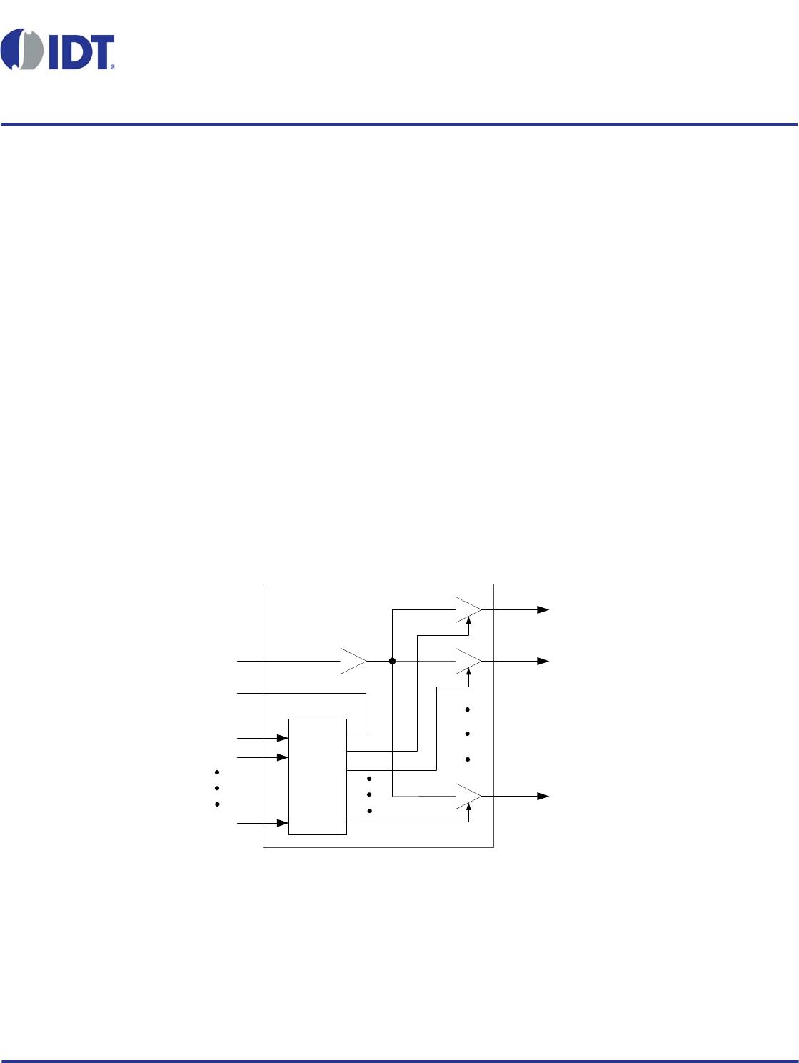
External Components
A minimum number of external components are required for proper operation. A decoupling capacitor of 0.01µF should be
connected between VDD on pin 1 and GND on pin 4, as close to the device as possible. A 33
series terminating resistor may
be used on each clock output if the trace is longer than 1 inch.
To achieve the low output skew that the 5PB12xx is capable of, careful attention must be paid to board layout. Essentially, all
four outputs must have identical terminations, identical loads and identical trace geometries. If they do not, the output skew will
be degraded. For example, using a 30
series termination on one output (with 33 on the others) will cause at least 15ps of
skew.
Absolute Maximum Ratings
Stresses above the ratings listed below can cause permanent damage to the 5PB12xx. These ratings, which are standard values
for IDT commercially rated parts, are stress ratings only. Functional operation of the device at these or any other conditions
above those indicated in the operational sections of the specifications is not implied. Exposure to absolute maximum rating
conditions for extended periods can affect product reliability. Electrical parameters are guaranteed only over the recommended
operating temperature range.
Item Rating
Supply Voltage, VDD 3.8V
Output Enable and All Inputs/Outputs -0.5 V to VDD + 0.5 V
Ambient Operating Temperature (extended) -40 to +105C
Storage Temperature -65 to +150C
Junction Temperature 125C
Soldering Temperature 260C
OE1 OE2 OE3 OE4 OE5 OE6 OE_OSC CLKOUT1 CLKOUT2 CLKOUT3 CLKOUT4 CLKOUT5 CLKOUT6
0 0 0 0 0 0 0 Hi-Z Hi-Z Hi-Z Hi-Z Hi-Z Hi-Z
1 0 0 0 0 0 1 CLOCK Hi-Z Hi-Z Hi-Z Hi-Z Hi-Z
1 1 0 0 0 0 1 CLOCK CLOCK Hi-Z Hi-Z Hi-Z Hi-Z
…………………………………
1 1 1 1 1 1 1 CLOCK CLOCK CLOCK CLOCK CLOCK CLOCK
Input Output