GSOT03C to GSOT36C
www.vishay.com
Vishay Semiconductors
Rev. 2.5, 07-Mar-16
4
Document Number: 85824
For technical questions, contact: ESDprotection@vishay.com
THIS DOCUMENT IS SUBJECT TO CHANGE WITHOUT NOTICE. THE PRODUCTS DESCRIBED HEREIN AND THIS DOCUMENT
ARE SUBJECT TO SPECIFIC DISCLAIMERS, SET FORTH AT www.vishay.com/doc?91000
ABSOLUTE MAXIMUM RATINGS GSOT24C
PARAMETER TEST CONDITIONS SYMBOL VALUE UNIT
Peak pulse current
Pin 1 to 3 or pin 2 to 3
acc. IEC 61000-4-5, t
p
= 8/20 μs; single shot
I
PPM
5A
Pin 1 to 2 or pin 2 to 1; pin 3 not connected
acc. IEC 61000-4-5, t
p
= 8/20 μs; single shot
5A
Peak pulse power
Pin 1 to 3 or pin 2 to 3
acc. IEC 61000-4-5, t
p
= 8/20 μs; single shot
P
PP
235 W
Pin 1 to 2 or pin 2 to 1; pin 3 not connected
acc. IEC 61000-4-5, t
p
= 8/20 μs; single shot
240 W
ESD immunity
Contact discharge acc. IEC 61000-4-2; 10 pulses
V
ESD
± 30 kV
Air discharge acc. IEC 61000-4-2; 10 pulses ± 30 kV
Operating temperature Junction temperature T
J
-55 to +150 °C
Storage temperature T
STG
-55 to +150 °C
ABSOLUTE MAXIMUM RATINGS GSOT36C
PARAMETER TEST CONDITIONS SYMBOL VALUE UNIT
Peak pulse current
Pin 1 to 3 or pin 2 to 3
acc. IEC 61000-4-5, t
p
= 8/20 μs; single shot
I
PPM
3.5 A
Pin 1 to 2 or pin 2 to 1; pin 3 not connected
acc. IEC 61000-4-5, t
p
= 8/20 μs; single shot
3.5 A
Peak pulse power
Pin 1 to 3 or pin 2 to 3
acc. IEC 61000-4-5, t
p
= 8/20 μs; single shot
P
PP
248 W
Pin 1 to 2 or pin 2 to 1; pin 3 not connected
acc. IEC 61000-4-5, t
p
= 8/20 μs; single shot
252 W
ESD immunity
Contact discharge acc. IEC 61000-4-2; 10 pulses
V
ESD
± 30 kV
Air discharge acc. IEC 61000-4-2; 10 pulses ± 30 kV
Operating temperature Junction temperature T
J
-55 to +150 °C
Storage temperature T
STG
-55 to +150 °C
GSOT03C to GSOT36C
www.vishay.com
Vishay Semiconductors
Rev. 2.5, 07-Mar-16
5
Document Number: 85824
For technical questions, contact: ESDprotection@vishay.com
THIS DOCUMENT IS SUBJECT TO CHANGE WITHOUT NOTICE. THE PRODUCTS DESCRIBED HEREIN AND THIS DOCUMENT
ARE SUBJECT TO SPECIFIC DISCLAIMERS, SET FORTH AT www.vishay.com/doc?91000
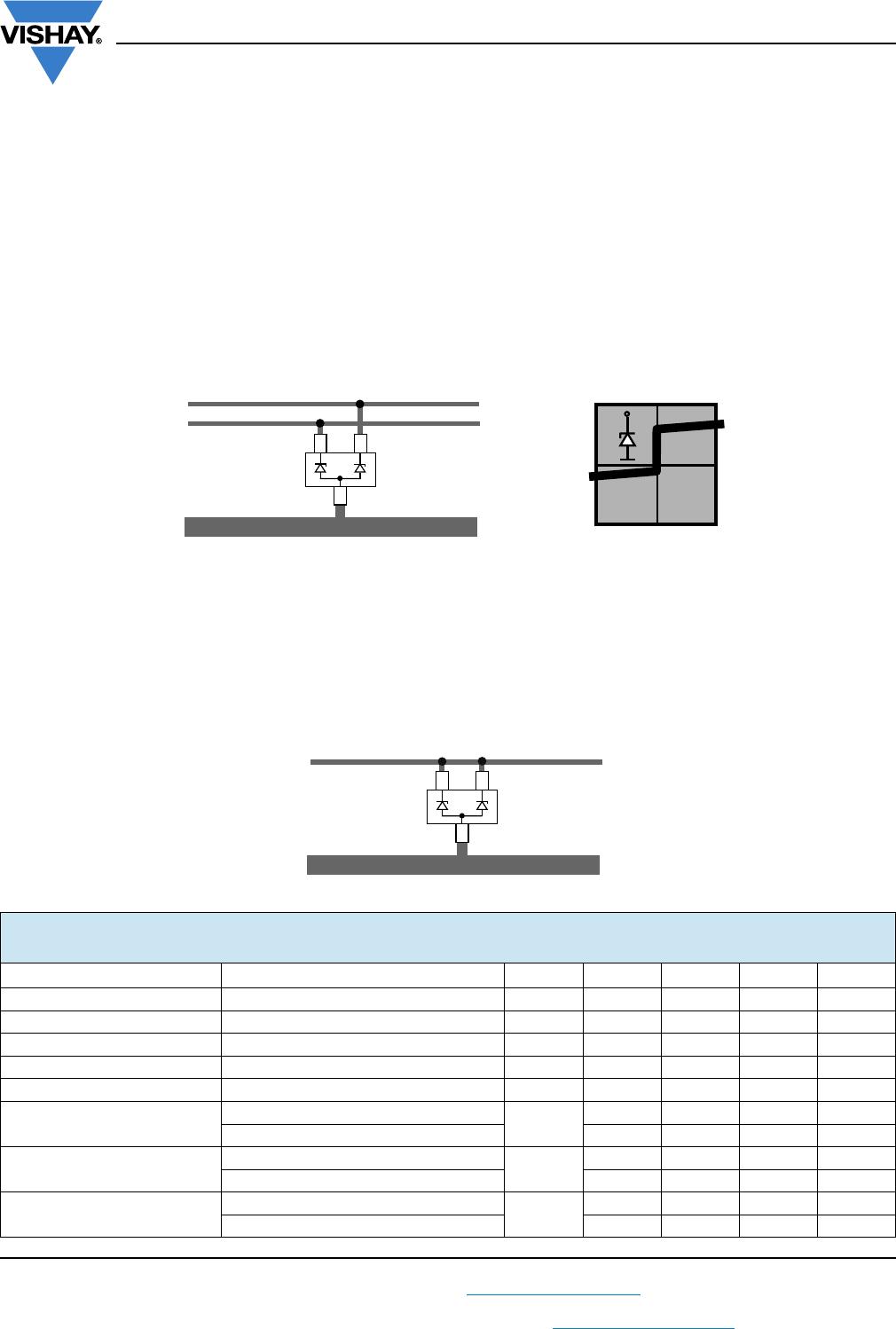
BiAs-MODE (2-line Bidirectional Asymmetrical protection mode)
With the GSOTxxC two signal- or data-lines (L1, L2) can be protected against voltage transients. With pin 3 connected to ground
and pin 1 and pin 2 connected to a signal- or data-line which has to be protected. As long as the voltage level on the data- or
signal-line is between 0 V (ground level) and the specified Maximum Reverse Working Voltage (V
RWM
) the protection diode
between pin 2 and pin 3 and between pin 1 and pin 3 offers a high isolation to the ground line. The protection device behaves
like an open switch.
As soon as any positive transient voltage signal exceeds the breakdown voltage level of the protection diode, the diode
becomes conductive and shorts the transient current to ground. Now the protection device behaves like a closed switch. The
Clamping Voltage (V
C
) is defined by the breakdown voltage (V
BR
) level plus the voltage drop at the series impedance (resistance
and inductance) of the protection diode.
Any negative transient signal will be clamped accordingly. The negative transient current is flowing in the forward direction
through the protection diode. The low Forward Voltage (V
F
) clamps the negative transient close to the ground level.
Due to the different clamping levels in forward and reverse direction the GSOTxxC clamping behavior is Bidirectional and
Asymmetrical (BiAs).
If a higher surge current or peak pulse current (I
PP
) is needed, both protection diodes in the GSOTxxC can also be used in
parallel in order to “double” the performance.
This offers:
double surge power = double peak pulse current (2 x I
PPM
)
half of the line inductance = reduced clamping voltage
half of the line resistance = reduced clamping voltage
double line capacitance (2 x C
D
)
double reverse leakage current (2 x I
R
)
ELECTRICAL CHARACTERISTICS GSOT03C (T
amb
= 25 °C unless otherwise specified)
between pin 1 to pin 3 or pin 2 to pin 3
PARAMETER TEST CONDITIONS/REMARKS SYMBOL MIN. TYP. MAX. UNIT
Protection paths Number of lines which can be protected N
channel
--2lines
Reverse stand-off voltage Max. reverse working voltage V
RWM
--3.3V
Reverse voltage at I
R
= 100 μA V
R
3.3 - - V
Reverse current at V
R
= 3.3 V I
R
- - 100 μA
Reverse breakdown voltage at I
R
= 1 mA V
BR
4.0 4.6 5.5 V
Reverse clamping voltage
at I
PP
= 1 A
V
C
-5.77.5V
at I
PP
= I
PPM
= 30 A - 10 12.3 V
Forward clamping voltage
at I
PP
= 1 A
V
F
-11.2V
at I
PP
= I
PPM
= 30 A - 4.5 - V
Capacitance
at V
R
= 0 V; f = 1 MHz
C
D
- 420 600 pF
at V
R
= 1.6 V; f = 1 MHz - 260 - pF
L1
L2
20358
2 1
3
Ground
BiAs
L1
20359
2 1
3
Ground
GSOT03C to GSOT36C
www.vishay.com
Vishay Semiconductors
Rev. 2.5, 07-Mar-16
6
Document Number: 85824
For technical questions, contact: ESDprotection@vishay.com
THIS DOCUMENT IS SUBJECT TO CHANGE WITHOUT NOTICE. THE PRODUCTS DESCRIBED HEREIN AND THIS DOCUMENT
ARE SUBJECT TO SPECIFIC DISCLAIMERS, SET FORTH AT www.vishay.com/doc?91000
ELECTRICAL CHARACTERISTICS GSOT04C (T
amb
= 25 °C unless otherwise specified)
between pin 1 to pin 3 or pin 2 to pin 3
PARAMETER TEST CONDITIONS/REMARKS SYMBOL MIN. TYP. MAX. UNIT
Protection paths Number of lines which can be protected N
channel
--2lines
Reverse stand-off voltage Max. reverse working voltage V
RWM
--4V
Reverse voltage at I
R
= 20 μA V
R
4--V
Reverse current at V
R
= 4 V I
R
--20μA
Reverse breakdown voltage at I
R
= 1 mA V
BR
56.17 V
Reverse clamping voltage
at I
PP
= 1 A
V
C
-7.59 V
at I
PP
= I
PPM
= 30 A - 11.2 14.3 V
Forward clamping voltage
at I
PP
= 1 A
V
F
-11.2V
at I
PP
= I
PPM
= 30 A - 4.5 - V
Capacitance
at V
R
= 0 V; f = 1 MHz
C
D
- 310 450 pF
at V
R
= 2 V; f = 1 MHz - 200 - pF
ELECTRICAL CHARACTERISTICS GSOT05C (T
amb
= 25 °C unless otherwise specified)
between pin 1 to pin 3 or pin 2 to pin 3
PARAMETER TEST CONDITIONS/REMARKS SYMBOL MIN. TYP. MAX. UNIT
Protection paths Number of lines which can be protected N
channel
--2lines
Reverse stand-off voltage Max. reverse working voltage V
RWM
--5V
Reverse voltage at I
R
= 10 μA V
R
5--V
Reverse current at V
R
= 5 V I
R
--10μA
Reverse breakdown voltage at I
R
= 1 mA V
BR
66.88 V
Reverse clamping voltage
at I
PP
= 1 A
V
C
-78.7V
at I
PP
= I
PPM
= 30 A - 12 16 V
Forward clamping voltage
at I
PP
= 1 A
V
F
-11.2V
at I
PP
= I
PPM
= 30 A - 4.5 - V
Capacitance
at V
R
= 0 V; f = 1 MHz
C
D
- 260 350 pF
at V
R
= 2.5 V; f = 1 MHz - 150 - pF
ELECTRICAL CHARACTERISTICS GSOT08C (T
amb
= 25 °C unless otherwise specified)
between pin 1 to pin 3 or pin 2 to pin 3
PARAMETER TEST CONDITIONS/REMARKS SYMBOL MIN. TYP. MAX. UNIT
Protection paths Number of lines which can be protected N
channel
--2lines
Reverse stand-off voltage Max. reverse working voltage V
RWM
--8V
Reverse voltage at I
R
= 5 μA V
R
8--V
Reverse current at V
R
= 8 V I
R
--5μA
Reverse breakdown voltage at I
R
= 1 mA V
BR
91011V
Reverse clamping voltage
at I
PP
= 1 A
V
C
- 10.7 13 V
at I
PP
= I
PPM
= 18 A - 15.2 19.2 V
Forward clamping voltage
at I
PP
= 1 A
V
F
-11.2V
at I
PP
= I
PPM
= 18 A - 3 - V
Capacitance
at V
R
= 0 V; f = 1 MHz
C
D
- 160 250 pF
at V
R
= 4 V; f = 1 MHz - 80 - pF

SMBJ48A

Mfr. #:
Manufacturer:
Littelfuse
Description:
TVS Diodes / ESD Suppressors 600W 48V 5% Uni-Directional
Lifecycle:
New from this manufacturer.
Delivery:
DHL FedEx Ups TNT EMS
Payment:
T/T Paypal Visa MoneyGram Western Union