24AA02E48/24AA025E48/24AA02E64/24AA025E64
DS20002124G-page 12 2008-2016 Microchip Technology Inc.
8.0 READ OPERATION
Read operations are initiated in the same way as write
operations, with the exception that the R/W
bit of the
slave address is set to ‘1’. There are three basic types
of read operations: current address read, random read
and sequential read.
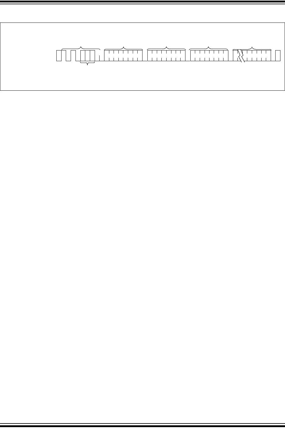
8.1 Current Address Read
The 24AA02XEXX contains an address counter that
maintains the address of the last word accessed,
internally incremented by one. Therefore, if the
previous access (either a read or write operation) was
to address ‘
n’, the next current address read operation
would access data from address
n+1. Upon receipt of
the slave address with R/W
bit set to ‘1’, the
24AA02XEXX issues an acknowledge and transmits
the 8-bit data word. The master will not acknowledge
the transfer, but generate a Stop condition, and the
24AA02XEXX discontinues transmission (Figure 8-1).
8.2 Random Read
Random read operations allow the master to access
any memory location in a random manner. To perform
this type of read operation, the word address must first
be set. This is accomplished by sending the word
address to the 24AA02XEXX as part of a write
operation. Once the word address is sent, the master
generates a Start condition following the acknowledge.
This terminates the write operation, but not before the
internal Address Pointer is set. The master then issues
the control byte again, but with the R/W
bit set to a ‘1’.
The 24AA02XEXX will then issue an acknowledge and
transmit the 8-bit data word. The master will not
acknowledge the transfer, but generate a Stop
condition, and the 24AA02XEXX will discontinue
transmission (Figure 8-2).
8.3 Sequential Read
Sequential reads are initiated in the same way as a
random read, except that once the 24AA02XEXX
transmits the first data byte, the master issues an
acknowledge as opposed to a Stop condition in a
random read. This directs the 24AA02XEXX to transmit
the next sequentially addressed 8-bit word (Figure 8-3).
To provide sequential reads, the 24AA02XEXX
contains an internal Address Pointer that is
incremented by one upon completion of each opera-
tion. This Address Pointer allows the entire memory
contents to be serially read during one operation.
8.4 Noise Protection
The 24AA02XEXX employs a VCC threshold detector
circuit which disables the internal erase/write logic if the
V
CC is below 1.5V at nominal conditions.
The SCL and SDA inputs have Schmitt Trigger and
filter circuits which suppress noise spikes to assure
proper device operation, even on a noisy bus.
FIGURE 8-1: CURRENT ADDRESS READ
SP
Bus Activity
Master
SDA Line
Bus Activity
S
T
O
P
Control
Byte
Data (n)
A
C
K
N
o
A
C
K
S
T
A
R
T
1
01
0
A2* A1*
A0*
1
Chip
Select
Bits
Note: * Bits A0, A1 and A2 are “don’t cares” for the 24AA02E48/24AA02E64.