24AA02E48/24AA025E48/24AA02E64/24AA025E64
DS20002124G-page 4 2008-2016 Microchip Technology Inc.
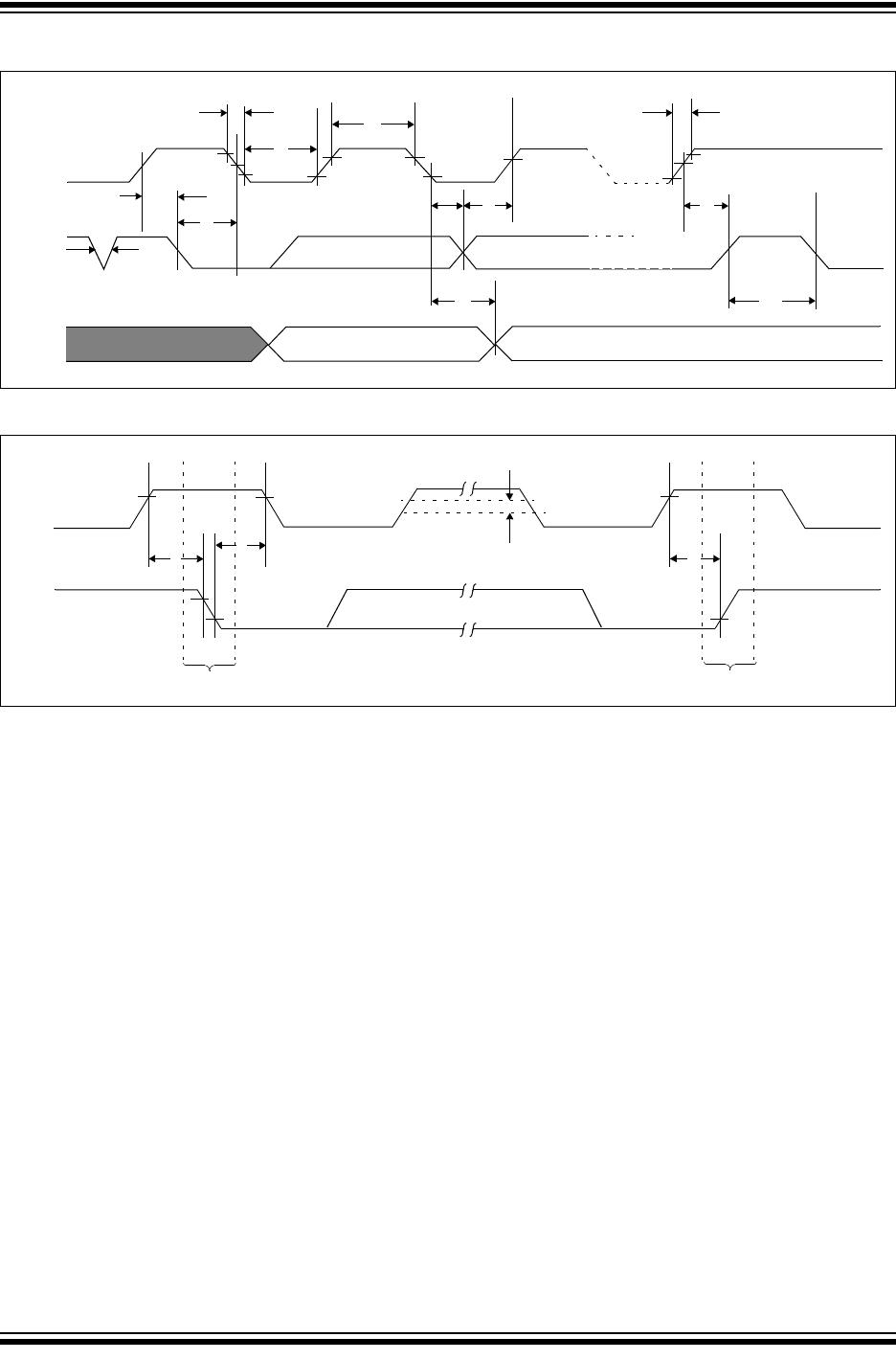
TABLE 1-2: AC CHARACTERISTICS
AC CHARACTERISTICS
Industrial (I): TA = -40°C to +85°C, VCC = +1.7V to +5.5V
Automotive (E): T
A = -40°C to +125°C, VCC = +1.7V to +5.5V
Param.
No.
Symbol Characteristic Min. Typ. Max. Units Conditions
1F
CLK Clock Frequency — — 400 kHz 2.5V VCC 5.5V
— — 100 kHz 1.7V V
CC 2.5V
2 THIGH Clock High Time 600 — — ns 2.5V VCC 5.5V
4000 — — ns 1.7V VCC 2.5V
3T
LOW Clock Low Time 1300 — — ns 2.5V VCC 5.5V
4700 — — ns 1.7V VCC 2.5V
4TR SDA and SCL Rise Time
(Note 1)
——300ns2.5V VCC 5.5V (Note 1)
— — 1000 ns 1.7V V
CC 2.5V (Note 1)
5TF SDA and SCL Fall Time — — 300 ns Note 1
6THD:STA Start Condition Hold Time 600 — — ns 2.5V VCC 5.5V
4000 — — ns 1.7V V
CC 2.5V
7TSU:STA Start Condition Setup Time 600 — — ns 2.5V VCC 5.5V
4700 — — ns 1.7V VCC 2.5V
8T
HD:DAT Data Input Hold Time 0 — — ns Note 2
9TSU:DAT Data Input Setup Time 100 — — ns 2.5V VCC 5.5V
250 — — ns 1.7V VCC 2.5V
10 T
SU:STO Stop Condition Setup Time 600 — — ns 2.5V VCC 5.5V
4000 — — ns 1.7V VCC 2.5V
11 TAA Output Valid from Clock
(Note 2)
——900ns2.5V VCC 5.5V
— — 3500 ns 1.7V V
CC 2.5V
12 TBUF Bus Free Time: Bus time
must be free before a new
transmission can start
1300 — — ns 2.5V VCC 5.5V
4700 — — ns 1.7V VCC 2.5V
13 TOF Output Fall Time from VIH
Minimum to V
IL Maximum
——250ns2.5V V
CC 5.5V
— — 250 ns 1.7V VCC 2.5V
14 T
SP Input Filter Spike
Suppression
(SDA and SCL pins)
— — 50 ns Notes 1 and 3
15 T
WC Write Cycle Time (byte or
page)
——5ms
16 Endurance 1M — — cycles 25°C (Note 4)
Note 1: Not 100% tested. C
B = total capacitance of one bus line in pF.
2: As a transmitter, the device must provide an internal minimum delay time to bridge the undefined region
(minimum 300 ns) of the falling edge of SCL to avoid unintended generation of Start or Stop conditions.
3: The combined T
SP and VHYS specifications are due to new Schmitt Trigger inputs which provide improved
noise spike suppression. This eliminates the need for a
TI specification for standard operation.
4: This parameter is not tested but ensured by characterization. For endurance estimates in a specific
application, please consult the Total Endurance™ Model which can be obtained from Microchip’s website
at www.microchip.com.