AD586
Rev. G | Page 9 of 16
00529-012
V
L
V
OUT
5V
50mV
1µS
Figure 13. Large-Scale Transient Response
00529-013
V
L
V
OUT
5V
1mV
2µS
Figure 14. Fine-Scale Setting for Transient Load
In some applications, a varying load may be both resistive and
capacitive in nature, or the load may be connected to the AD586
by a long capacitive cable.
Figure 15 and Figure 16 display the output amplifier
characteristics driving a 1000 pF, 0 mA to 10 mA load.
AD586
V
L
5V
0V
V
OUT
C
L
1000pF
500
3.5V
00529-014
Figure 15. Capacitive Load Transient Response Test Circuit
00529-015
C
L
= 0
C
L
= 1000pF
5V
200mV
1µS
Figure 16. Output Response with Capacitive Load
LOAD REGULATION
The AD586 has excellent load regulation characteristics. Figure 17
shows that varying the load several mA changes the output by a
few µV. The AD586 has somewhat better load regulation per-
formance sourcing current than sinking current.
–6 –4 –2
246810
LOAD (mA)
0
–500
–1000
500
1000
V
OUT
(µV)
00529-016
Figure 17. Typical Load Regulation Characteristics
TEMPERATURE PERFORMANCE
The AD586 is designed for precision reference applications
where temperature performance is critical. Extensive tempera-
ture testing ensures that the device maintains a high level of
performance over the operating temperature range.
Some confusion exists with defining and specifying reference
voltage error over temperature. Historically, references have
been characterized using a maximum deviation per degree
Celsius, that is, ppm/°C. However, because of nonlinearities in
temperature characteristics that originated in standard Zener
references (such as “S type characteristics), most manufacturers
have begun to use a maximum limit error band approach to
specify devices. This technique involves measuring the output at
three or more different temperatures to specify an output volt-
age error band.
AD586
Rev. G | Page 10 of 16
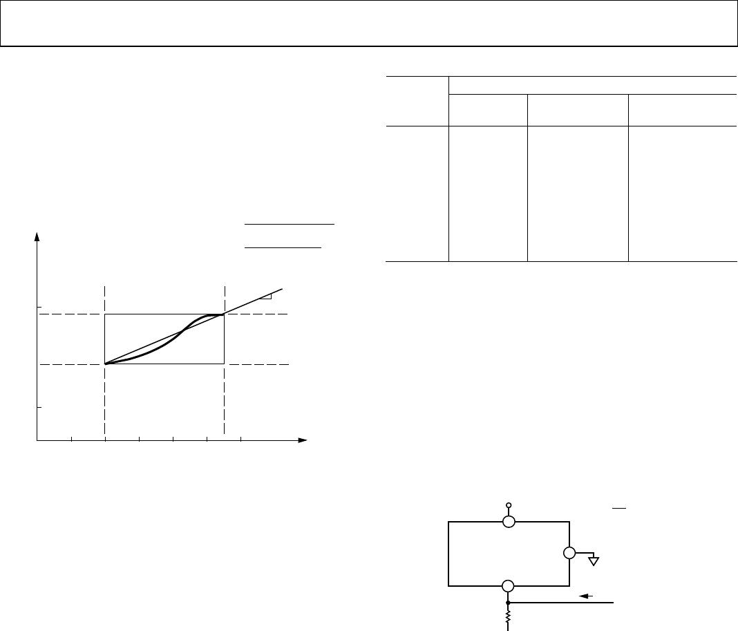
Figure 18 shows the typical output voltage drift for the AD586L
and illustrates the test methodology. The box in Figure 18 is
bounded on the sides by the operating temperature extremes
and on the top and the bottom by the maximum and minimum
output voltages measured over the operating temperature
range. The slope of the diagonal drawn from the lower left to
the upper right corner of the box determines the performance
grade of the device.
–20 0 20 40 60 80
5
.003
5.000
TEMPERATURE (°C)
V
MIN
V
MAX
V
MAX
–V
MIN
(T
MAX
–T
MIN
) × 5 × 10
–6
SLOPE
T
MIN
T
MAX
SLOPE = T.C. =
=
=
4.3ppm/°C
5.0027 – 5.0012
(70°C – 0) × 5 × 10
–6
00625-017
Figure 18. Typical AD586L Temperature Drift
Each AD586J, AD586K, and AD586L grade unit is tested at 0°C,
25°C, and 70°C. Each AD586SQ and AD586TQ grade unit is
tested at −55°C, +25°C, and +125°C. This approach ensures that
the variations of output voltage that occur as the temperature
changes within the specified range will be contained within a
box whose diagonal has a slope equal to the maximum specified
drift. The position of the box on the vertical scale will change
from device to device as initial error and the shape of the curve
vary. The maximum height of the box for the appropriate tem-
perature range and device grade is shown in Table 5. Dupli-
cation of these results requires a combination of high accuracy
and stable temperature control in a test system. Evaluation of
the AD586 will produce a curve similar to that in Figure 18, but
output readings could vary depending on the test methods and
equipment used.
Table 5. Maximum Output Change in mV
Maximum Output Change (mV)
Device
Grade
0°C to 70°C −40°C to +85°C −55°C to +125°C
AD586J 8.75
AD586K 5.25
AD586L 1.75
AD586M 0.70
AD586A 9.37
AD586B 3.12
AD586S 18.00
AD586T 9.00
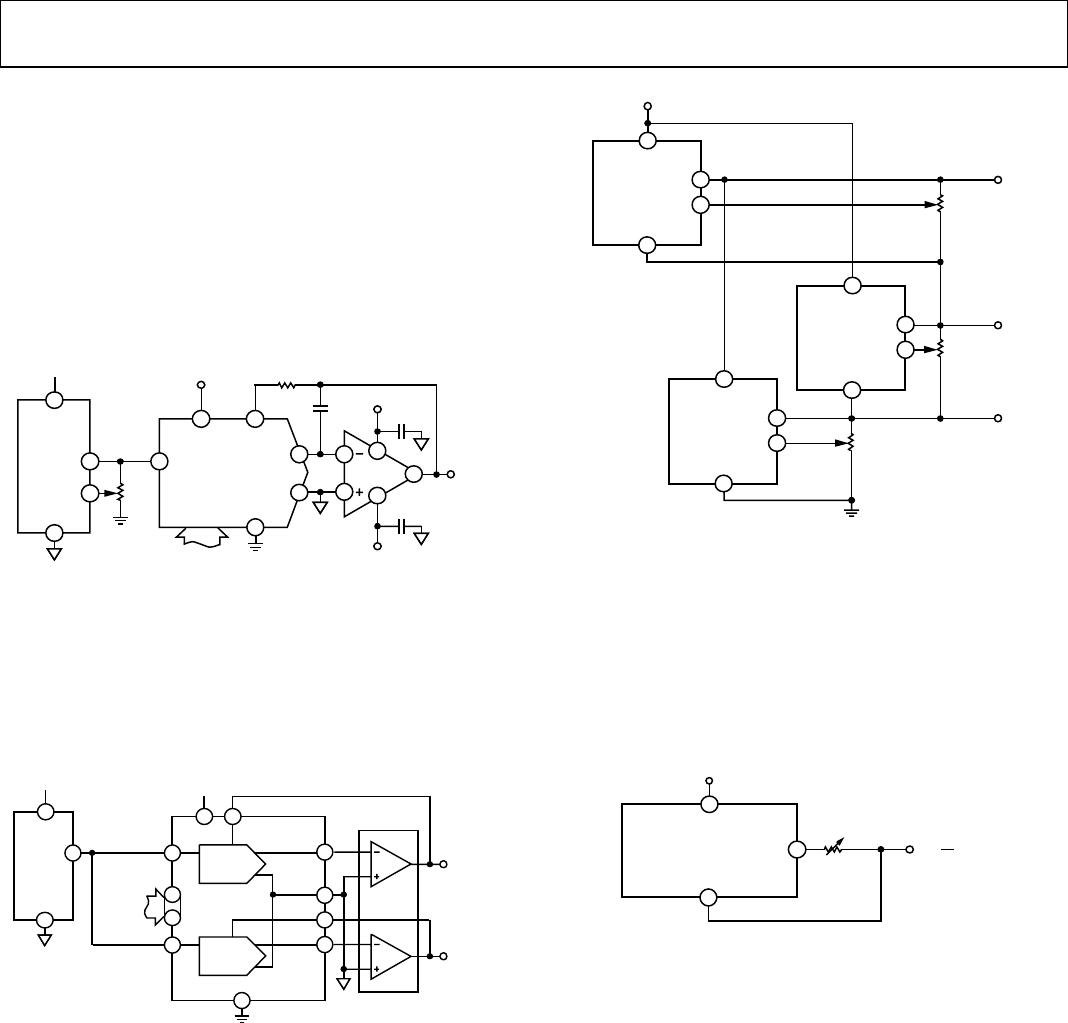
NEGATIVE REFERENCE VOLTAGE FROM AN AD586
The AD586 can be used to provide a precision −5.000 V output,
as shown in Figure 19. The V
IN
pin is tied to at least a 6 V supply,
the output pin is grounded, and the AD586 ground pin is con-
nected through a resistor, R
S
, to a −15 V supply. The −5 V output
is now taken from the ground pin (Pin 4) instead of V
OUT
. It is
essential to arrange the output load and the supply resistor, R
S,
so that the net current through the AD586 is between 2.5 mA
and 10.0 mA. The temperature characteristics and long-term
stability of the device will be essentially the same as that of a
unit used in the standard +5 V output configuration.
AD586
GND
+6V +30V
2.5mA < I
L
< 10mA
10V
R
S
–5V
R
S
V
OUT
V
IN
I
L
–15V
2
4
6
00529-018
Figure 19. AD586 as a Negative 5 V Reference
USING THE AD586 WITH CONVERTERS
The AD586 is an ideal reference for a wide variety of 8-, 12-, 14-,
and 16-bit ADCs and DACs. Several representative examples are
explained in the following sections.
AD586
Rev. G | Page 11 of 16
5 V REFERENCE WITH MULTIPLYING
CMOS DACs OR ADCs
The AD586 is ideal for applications with 10- and 12-bit
multiplying CMOS DACs. In the standard hookup, as shown
in Figure 20, the AD586 is paired with the AD7545 12-bit
multiplying DAC and the AD711 high speed BiFET op amp.
The amplifier DAC configuration produces a unipolar 0 V to
−5 V output range. Bipolar output applications and other
operating details can be found in the individual product data
sheets.
AD586
GND
V
OUT
V
IN
AD711K
0.1µF
0.1µF
–15V
0V TO–5V
+15V
OUT 1
AGND
DGND
DB11TO DB0
C1
33pF
R2
68
R
FB
+15V
V
DD
AD7545K
V
REF
10k
V
OUT
TRIM
+15V
2018
196
5
4
2
3
1 2
7
4
6
3
2
00529-019
Figure 20. Low Power 12-Bit CMOS DAC Application
The AD586 can also be used as a precision reference for multi-
ple DACs. Figure 21 shows the AD586, the AD7628 dual DAC,
and the AD712 dual op amp hooked up for single-supply opera-
tion to produce 0 V to −5 V outputs. Because both DACs are on
the same die and share a common reference and output op
amps, the DAC outputs will exhibit similar gain TCs.
AD586
GND
AD712
OUT A
DGND
AGND
DAC A
DB0
DB7
DATA
INPUTS
OUT B
DAC B
RFB B
RFB A
V
REF
A
V
REF
B
AD7628
V
IN
V
OUT
A=
0TO–5V
V
OUT
B=
0TO–5V
V
OUT
+15V
+15V
6 4
4
7
14
2
5
317
1
19
20
2
4
00529-020
Figure 21. AD586 as a 5 V Reference for a CMOS
STACKED PRECISION REFERENCES FOR
MULTIPLE VOLTAGES
Often, a design requires several reference voltages. Three
AD586s can be stacked, as shown in Figure 22, to produce
5.000 V, 10.000 V, and 15.000 V outputs. This scheme can be
extended to any number of AD586s, provided the maximum
load current is not exceeded. This design provides the addi-
tional advantage of improved line regulation on the 5.0 V
output. Changes in V
IN
of 18 V to 50 V produce output changes
that are below the noise level of the references.
22V TO 46V
AD586
GND
V
OUT
V
IN
TRIM
10k
AD586
GND
V
OUT
V
IN
TRIM
AD586
GND
V
OUT
V
IN
TRIM
10k
10k
15V
10V
5V
2
4
5
6
2
4
5
6
2
4
5
6
00529-021
Figure 22. Multiple AD586s Stacked for Precision 5 V, 10 V, and 15 V Outputs
PRECISION CURRENT SOURCE
The design of the AD586 allows it to be easily configured as a
current source. By choosing the control resistor R
C
in Figure 23,
the user can vary the load current from the quiescent current
(typically, 2 mA) to approximately 10 mA. The compliance volt-
age of this circuit varies from about 5 V to 21 V, depending on
the value of V
IN
.
AD586
GND
V
OUT
V
IN
5V
R
C
I
L
= + I
BIAS
+V
IN
R
C
(500 MIN)
2
4
6
00529-022
Figure 23. Precision Current Source
PRECISION HIGH CURRENT SUPPLY
For higher currents, the AD586 can easily be connected to a
power PNP or power Darlington PNP device. The circuit in
Figure 24 and Figure 25 can deliver up to 4 amps to the load.
The 0.1 µF capacitor is required only if the load has a significant
capacitive component. If the load is purely resistive, improved
high frequency supply rejection results can be obtained by
removing the capacitor.

AD586JNZ

Mfr. #:
Manufacturer:
Analog Devices Inc.
Description:
Voltage References IC HI PREC 5V REF
Lifecycle:
New from this manufacturer.
Delivery:
DHL FedEx Ups TNT EMS
Payment:
T/T Paypal Visa MoneyGram Western Union