AD586
Rev. G | Page 3 of 16
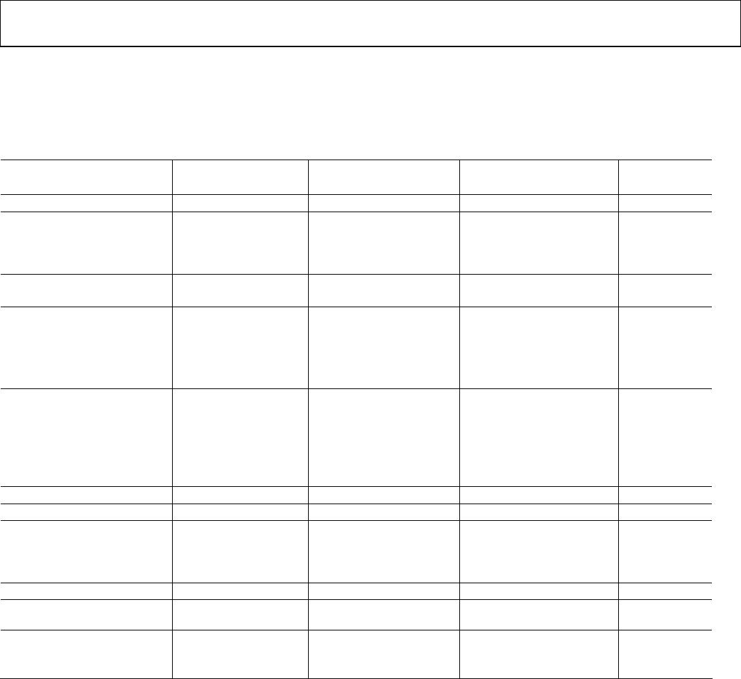
SPECIFICATIONS
AD586J, AD586K/AD586A, AD586L/AD586B
@ T
A
= 25°C, V
IN
= 15 V, unless otherwise noted. Specifications in boldface are tested on all production units at final electrical test. Results
from those tests are used to calculate outgoing quality levels. All minimum and maximum specifications are guaranteed, although only
those shown in boldface are tested on all production units, unless otherwise specified.
Table 1.
AD586J AD586K/AD586A AD586L/AD586B
Parameter Min Typ Max Min Typ Max Min Typ Max Unit
OUTPUT VOLTAGE 4.980 5.020 4.995 5.005 4.9975 5.0025 V
OUTPUT VOLTAGE
DRIFT
1
0°C to 70°C 25 15 5 ppm/°C
−55°C to +125°C ppm/°C
GAIN ADJUSTMENT
+6
+6
+6
%
−2 −2 −2 %
LINE REGULATION
1
10.8 V < + V
IN
< 36 V
T
MIN
to T
MAX
±100
±100
±100
µV/V
11.4 V < +V
IN
< 36 V
T
MIN
to T
MAX
µV/V
LOAD REGULATION
1
Sourcing 0 mA < I
OUT
< 10 mA
25°C
100
100
100
µV/mA
T
MIN
to T
MAX
100
100
100
µV/mA
Sinking −10 mA < I
OUT
< 0 mA
25°C
400
400
400
µV/mA
QUIESCENT CURRENT 2
3
2
3
2
3
mA
POWER CONSUMPTION 30 30 30 mW
OUTPUT NOISE
0.1 Hz to 10 Hz 4 4 4 µV p-p
Spectral Density, 100 Hz 100 100 100 nV/√Hz
LONG-TERM STABILITY 15 15 15 ppm/1000 hr
SHORT-CIRCUIT
CURRENT-TO-GROUND
45
60
45
60
45
60
mA
TEMPERATURE RANGE
Specified Performance
2
0 70 0
40
(K grade)
(A grade)
70
+85
0
40
(L grade)
(B grade)
70
+85
°C
°C
Operating Performance
3
−40 +85 −40 +85 −40 +85 °C
1
Maximum output voltage drift is guaranteed for all packages and grades. CERDIP packaged parts are also 100°C production tested.
2
Lower row shows specified performance for A and B grades.
3
The operating temperature range is defined as the temperature extremes at which the device will still function. Parts may deviate from their specified performance
outside their specified temperature range.
AD586
Rev. G | Page 4 of 16
AD586M, AD586S, AD586T
@ T
A
= 25°C, V
IN
= 15 V, unless otherwise noted. Specifications in boldface are tested on all production units at final electrical test. Results
from those tests are used to calculate outgoing quality levels. All minimum and maximum specifications are guaranteed, although only
those shown in boldface are tested on all production units, unless otherwise specified.
Table 2.
AD586M AD586S AD586T
Parameter Min Typ Max Min Typ Max Min Typ Max Unit
OUTPUT VOLTAGE 4.998 5.002 4.990 5.010 4.9975 5.0025 V
OUTPUT VOLTAGE
DRIFT
1
0°C to 70°C 2 ppm/°C
−55°C to +125°C 20 10 ppm/°C
GAIN ADJUSTMENT
+6
+6
+6
%
−2 −2 −2 %
LINE REGULATION
1
10.8 V < +V
IN
< 36 V
T
MIN
to T
MAX
±100
µV/V
11.4 V < +V
IN
< 36 V
T
MIN
to T
MAX
±150
±150
µV/V
LOAD REGULATION
1
Sourcing 0 mA < I
OUT
< 10 mA
25°C
100
150
150
µV/mA
T
MIN
to T
MAX
100
150
150
µV/mA
Sinking −10 mA < I
OUT
< 0 mA
25°C
400 400 400 µV/mA
QUIESCENT CURRENT 2
3
2
3
2
3
mA
POWER CONSUMPTION 30 30 30 mW
OUTPUT NOISE
0.1 Hz to 10 Hz 4 4 4 µV p-p
Spectral Density,
100 Hz
100 100 100 nV/√Hz
LONG-TERM STABILITY 15 15 15 ppm/1000 hr
SHORT-CIRCUIT
CURRENT-TO-GROUND
45
60
45
60
45
60
mA
TEMPERATURE RANGE
Specified Performance
2
0 70 −55 +125 −55 +125 °C
Operating Performance
3
−40 +85 −55 +125 −55 +125 °C
1
Maximum output voltage drift is guaranteed for all packages and grades. CERDIP packaged parts are also 100°C production tested.
2
Lower row shows specified performance for A and B grades.
3
The operating temperature range is defined as the temperature extremes at which the device will still function. Parts may deviate from their specified performance
outside their specified temperature range.
AD586
Rev. G | Page 5 of 16
ABSOLUTE MAXIMUM RATINGS
Table 3.
Parameter Rating
V
IN
to Ground 36 V
Power Dissipation (25°C) 500 mW
Storage Temperature −65°C to +150°C
Lead Temperature (Soldering, 10 sec) 300°C
Package Thermal Resistance
θ
JC
22°C/W
θ
JA
110°C/W
Output Protection
Output safe for indefinite
short to ground or V
IN
.
Stresses above those listed under Absolute Maximum Ratings
may cause permanent damage to the device. This is a stress
rating only; functional operation of the device at these or any
other conditions above those indicated in the operational
section of this specification is not implied. Exposure to absolute
maximum rating conditions for extended periods may affect
device reliability.
ESD CAUTION
ESD (electrostatic discharge) sensitive device. Electrostatic charges as high as 4000 V readily accumulate on the
human body and test equipment and can discharge without detection. Although this product features
proprietary ESD protection circuitry, permanent damage may occur on devices subjected to high energy
electrostatic discharges. Therefore, proper ESD precautions are recommended to avoid performance
degradation or loss of functionality.

AD586JNZ

Mfr. #:
Manufacturer:
Analog Devices Inc.
Description:
Voltage References IC HI PREC 5V REF
Lifecycle:
New from this manufacturer.
Delivery:
DHL FedEx Ups TNT EMS
Payment:
T/T Paypal Visa MoneyGram Western Union