ADA-4743-TR2G

ADA-4743
Silicon Bipolar Darlington Ampli er
Data Sheet
Description
Avago Technologies ADA-4743 is an economical, easy-to-
use, general purpose silicon bipolar RFIC gain block am-
pli ers housed in a 4-lead SC-70 (SOT-343) surface mount
plastic package which requires only half the board space
of a SOT-143 package.
The Darlington feedback structure provides inherent
broad bandwidth performance, resulting in useful oper-
ating frequency up to 2.5 GHz. This is an ideal device for
small-signal gain cascades or IF ampli cation.
ADA-4743 is fabricated using Avagos HP25 silicon bi-
polar process, which employs a double-di used single
polysilicon process with self-aligned submicron emitter
geometry. The process is capable of simultaneous high fT
and high NPN breakdown (25 GHz fT at 6V BVCEO). The
process utilizes industry standard device oxide isolation
technologies and submicron aluminum multilayer inter-
connect to achieve superior performance, high uniformi-
ty, and proven reliability.
Attention:
Observe precautions for handling
electrostatic sensitive devices.
ESD Machine Model (Class A)
ESD Human Body Model (Class 1B)
Refer to Avago Application Note A004R:
Electrostatic Discharge Damage and Control.
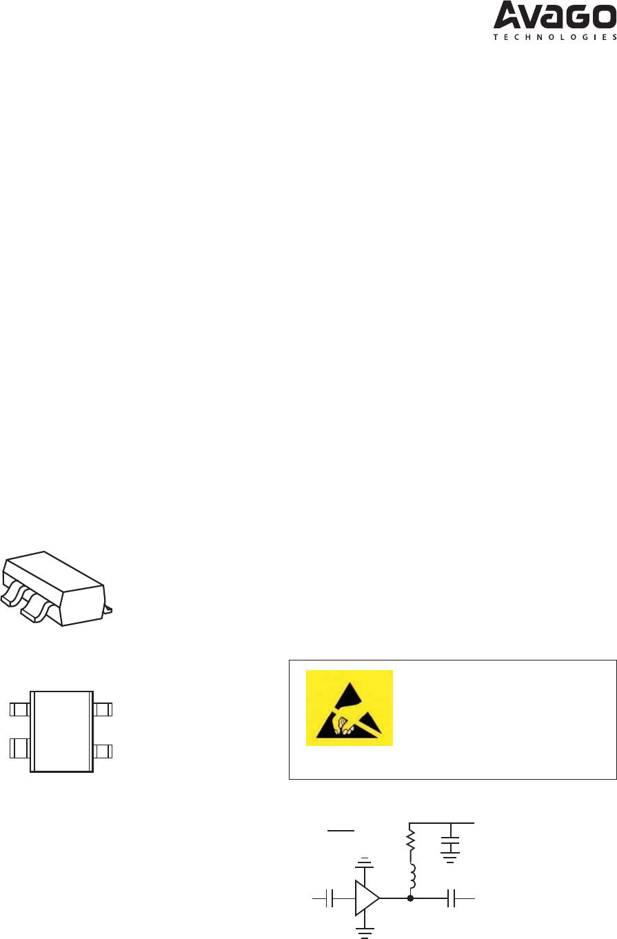
SOT-343 Surface Mount Package
Pin Connections and Package Marking
RFin
3Tx
GND
RFout
& Vd
GND
Note:
Top View. Package marking provides orientation and identification.
“3T” = Device Code
“x” = Date code character
identifies month of manufacture.
Features
Small Signal gain amplifier
Operating frequency DC – 2.5 GHz
Unconditionally stable
50 Ohms input & output
Flat, Broadband Frequency Response up to 1 GHz
Operating Current: 40 to 80 mA
Industry standard SOT-343 package
Lead-free option available
Specifications
900 MHz, 3.8V, 60 mA (typ.)
16.5 dB associated gain
17.1 dBm P
1dB
32.6 dBm OIP
3
4.2 dB noise figure
VSWR < 2 throughput operating frequency
Single supply, typical I
d
= 60 mA
Applications
Cellular/PCS/WLL base stations
Wireless data/WLAN
Fiber-optic systems
ISM
C
block
C
block
C
bypass
R
c
V
CC
=
5
V
V
d
= 3.8 V
RFC
RF
input
RF
output
3Tx
R
c
=
V
cc
- V
d
I
d
Typical Biasing Configuration
2
ADA-4743 Absolute Maximum Ratings
[1]
Absolute
Symbol Parameter Units Maximum
I
d
Device Current mA 90
P
diss
Total Power Dissipation
[2]
mW 370
P
in max.
RF Input Power dBm 20
T
j
Channel Temperature °C 150
T
STG
Storage Temperature °C -65 to 150
θ
jc
Thermal Resistance
[3]
°C/W 163
Notes:
1. Operation of this device above any one of
these parameters may cause permanent
damage.
2. Ground lead temperature is 25°C.
Derate 6.1 mW/°C for TL >89°C .
3. Junction-to-case thermal resistance
measured using 150°C Liquid Crystal
Measurement method.
ADA-4743 Electrical Specifications
T
A
= 25°C, Zo=50Ω, Pin = -25 dBm, I
d
= 60 mA (unless specified otherwise)
Symbol Parameter and Test Condition: Frequency Units Min. Typ. Max. Std. Dev.
I
d
= 60 mA, Zo = 50Ω
V
d
Device Voltage I
d
= 60 mA V 3.3 3.8 4.3
Gp Power Gain (|S
21
|
2
100 MHz dB 16.6
900 MHz
[1,2]
15 16.5 18
ΔGp Gain Flatness 100 to 900 MHz dB 0.5
0.1 to 2 GHz 1.5
F
3dB
3 dB Bandwidth GHz 4
VSWR
in
Input Voltage Standing Wave Ratio 0.1 to 6 GHz 1.7:1
VSWR
out
Output Voltage Standing Wave Ratio 0.1 to 6 GHz 1.5:1
NF 50Ω Noise Figure 100 MHz dB 4.1 0.11
900 MHz
[1,2]
4.2 0.16
P
1dB
Output Power at 1dB Gain Compression 100 MHz dBm 17.7
900 MHz
[1,2]
17.1
OIP
3
Output 3
rd
Order Intercept Point 100 MHz
[3]
dBm 33.4
900 MHz
[1,2,3]
32.6
DV/dT Device Voltage Temperature Coefficient mV/°C -4.9
Notes:
1. Typical value determined from a sample size of 500 parts from 3 wafers.
2. Measurement obtained using production test board described in the block diagram below.
3. I) 900 MHz OIP
3
test condition: F1 = 900 MHz, F2 = 905 MHz and Pin = -25 dBm per tone.
II) 100 MHz OIP
3
test condition: F1 = 100 MHz, F2 = 105 MHz and Pin = -25 dBm per tone.
Block diagram of 900 MHz production test board used for V
d
, Gain, P
1dB
, OIP
3
, and NF measurements.
Circuit losses have been de-embedded from actual measurements.
Input
50 Ohm
Transmission
(0.5 dB loss)
DUT
50 Ohm
Transmission
including Bias
(0.5 dB loss)
Output
3
ADA-4743 Typical Performance Curves (at 25°C, unless specified otherwise)
Product Consistency Distribution Charts at 900 MHz, I
d
= 60 mA
Notes:
1. Statistics distribution determined from a sample size of 500 parts taken from 3 different wafers.
2. Future wafers allocated to this product may have typical values anywhere between the minimum and maximum specification limits.
GAIN (dB)
15 1
8
1615.5 1716.5
17.5
300
250
200
150
100
50
0
Figure 1. Gain distribution @ 60 mA.
LSL=15, Nominal=16.5, USL = 18
V
d
(V)
3.3 4.3
3.5 3.7 3.9 4.1
240
200
160
120
80
40
0
Figure 2. V
d
distribution @ 60 mA.
LSL=3.3, Nominal=3.8, USL = 4.3
FREQUENCY (GHz)
Figure 3. Gain vs. Frequency at I
d
= 60 mA.
GAIN (dB)
FREQUENCY (GHz)
Figure 4. P
1dB
vs. Frequency at I
d
=60 mA.
FREQUENCY (GHz)
Figure 5. OIP
3
vs. Frequency at I
d
=60 mA.
FREQUENCY (GHz)
Figure 6. NF vs. Frequency at I
d
=60 mA.
V
d
(V)
Figure 7. I
d
vs. V
d
and Temperature.
I
d
(mA)
Figure 8. Gain vs. I
d
and Temperature at 900 MHz.
GAIN (dB)
P
1dB
(dBm)
OIP
3
(dBm)
NF (dB)
I
d
(mA)
0621 3 54
20
15
10
5
0
0621 3 54
20
15
10
5
0
0621 3 54
35
30
25
20
15
10
0621 3 54
6
5
4
3
2
0521 3 4
90
80
70
60
50
40
30
20
10
0
-40°C
25°C
85°C
0 10020 40 8060
17
16.5
16
15.5
15
14.5
14
-40°C
25°C
85°C

ADA-4743-TR2G

Mfr. #:
Manufacturer:
Broadcom / Avago
Description:
RF Amplifier DC - 2.5 GHz 16.5dB
Lifecycle:
New from this manufacturer.
Delivery:
DHL FedEx Ups TNT EMS
Payment:
T/T Paypal Visa MoneyGram Western Union

Products related to this Datasheet