DATASHEET
Photolink- Fiber Optic Receiver
EAPLRBA1
Copyright © 2010, Everlight Americas Inc. All Rights Reserved. Release Date : 11.13.2012. Issue No: 1
www.everlightamericas .com
1. Above specification may be changed without notice. EVERLIGHT Americas will reserve authority on material
change for above specification.
2. .When using this product, please observe the absolute maximum ratings and the instructions for using outlined
in these specification sheets. EVERLIGHT Americas assumes no responsibility for any damage resulting from
use of the product which does not comply with the absolute maximum ratings and the instructions included in
these specification sheets.
3. These specification sheets include materials protected under copyright of EVERLIGHT Americas corporation.
Please don’t reproduce or cause anyone to reproduce them without EVERLIGHT Americas’s consent.
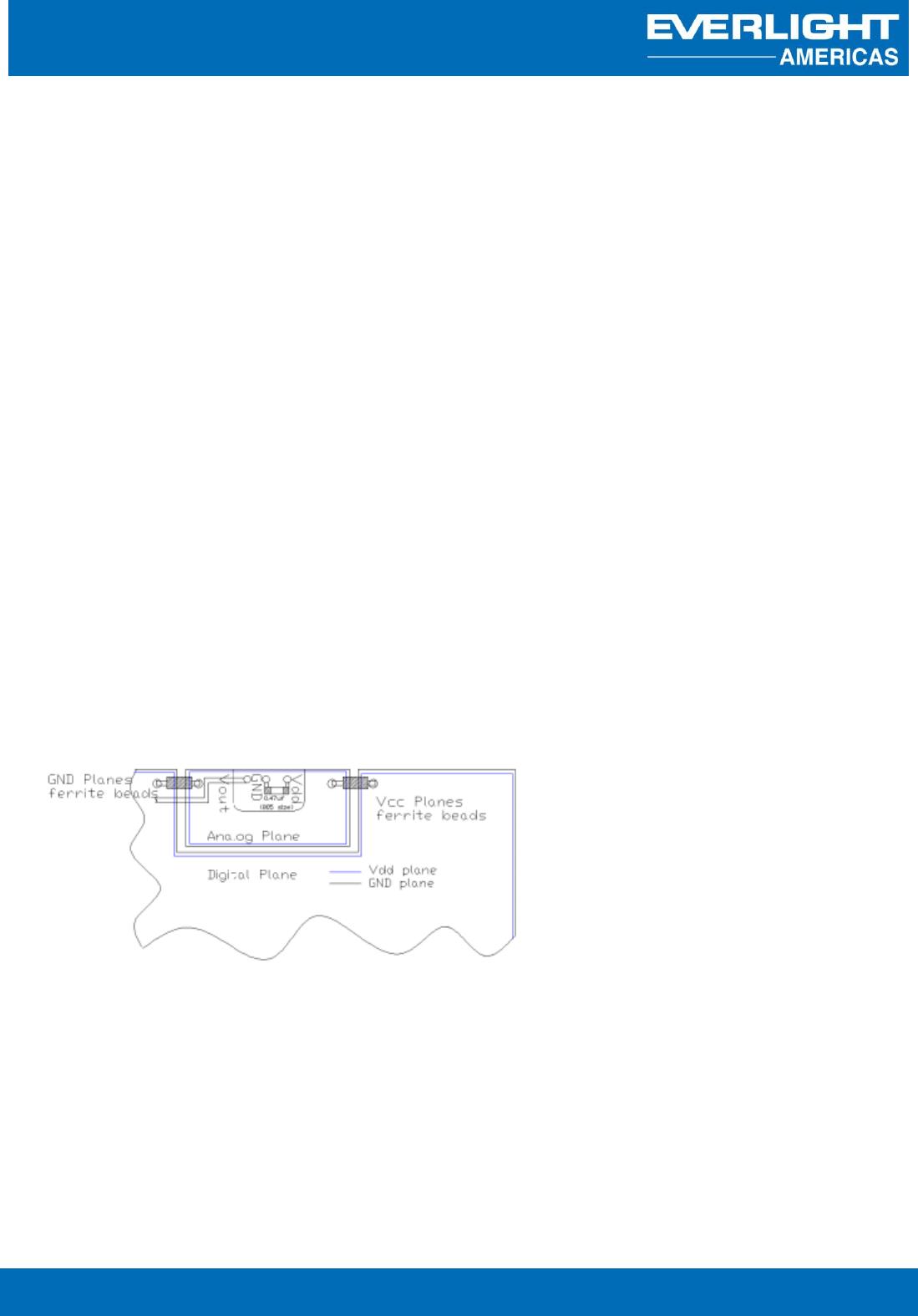
Application Notes: EAPLRBA1 PCB layout for motherboard integration
To achieve better jitter and low input optical power performances, several PCB layout guidelines must be followed.
These guidelines ensure the most reliable EAPLRBA1 POF performance for the motherboard integration. Failed to
implement these PCB guidelines may affect the EAPLRBA1 jitter and low input power performances.
1. Careful decoupling of the power supplies is very important. Place a 0.1uf surface mount (size 805 or smaller)
capacitor as close as (less than 2cm) to the POF Vdd and Gnd leads. The 0.1uf act as a low impedance path to
ground for any stray high frequency transient noises.
2. To reduce the digital noises form the digital IC on the motherboard, the planar capacitance formed by an
isolated Vcc and Gnd planes is critical. The POF device must be mounted directly on these two planes to
reduce the lead parasitic inductance.
3. The isolated Vdd and Gnd planes must be connected to the main Vcc and Gnd (digital) planes at a single point
using ferrite beads. The beads are used to block the high frequency noises from the digital planes while still
allowing the DC connections between the planes