ICS661
PRECISION AUDIO CLOCK SOURCE CLOCK SYNTHESIZER
IDT™ / ICS™
PRECISION AUDIO CLOCK SOURCE 3
ICS661 REV F 051310
Application Information
Series Termination Resistor
Clock output traces should use series termination. To series
terminate a 50Ω trace (a commonly used trace impedance),
place a 33Ω resistor in series with the clock line, as close to
the clock output pin as possible. The nominal impedance of
the clock output is 20Ω.
Decoupling Capacitors
As with any high performance mixed-signal IC, the ICS661
must be isolated from system power supply noise to perform
optimally.
Decoupling capacitors of 0.01µF must be connected
between each VDD and the PCB ground plane. To further
guard against interfering system supply noise, the ICS661
should use one common connection to the PCB power
plane as shown in the diagram on the next page. The ferrite
bead and bulk capacitor help reduce lower frequency noise
in the supply that can lead to output clock phase modulation.
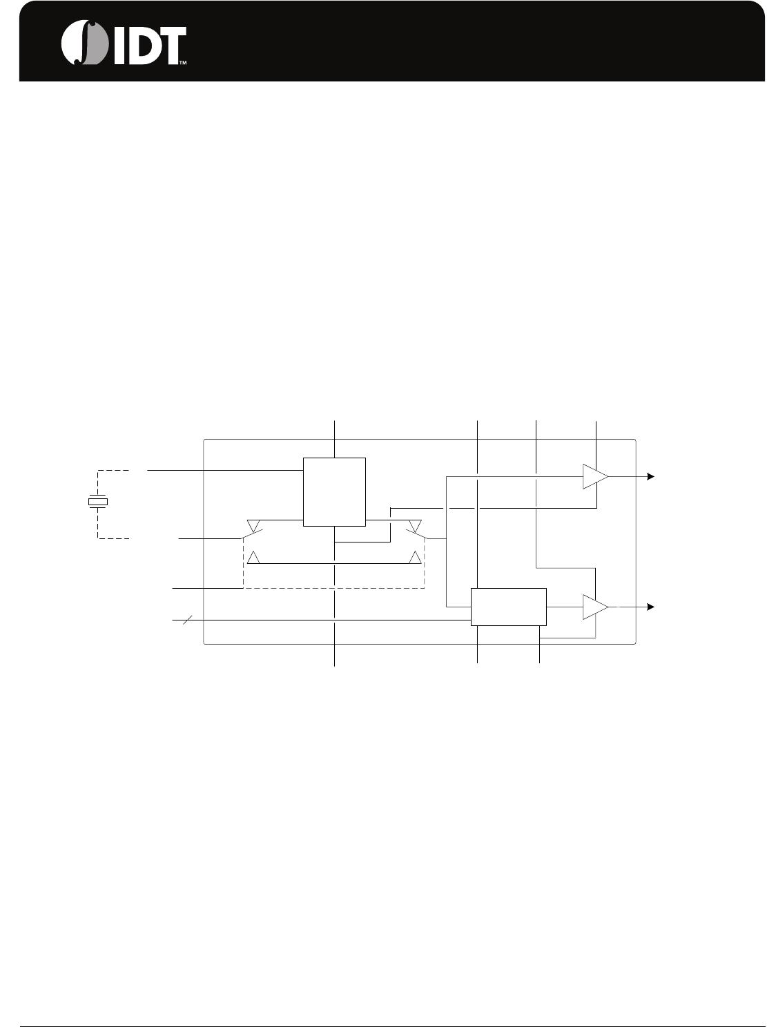
Recommended Power Supply Connection for
Optimal Device Performance
All power supply pins must be connected to the same
voltage, except VDDR and VDDO may be connected to a
lower voltage in order to change the output level. If the
reference output is not used, ground VDDR.
Crystal Load Capacitors
If a crystal is used, the device crystal connections should
include pads for capacitors from X1 to ground and from X2
to ground. These capacitors are used to adjust the stray
capacitance of the board to match the nominally required
crystal load capacitance. To reduce possible noise pickup,
use very short PCB traces (and no vias) been the crystal
and device.
The value of the load capacitors can be roughly determined
by the formula C = 2(C
L
- 6) where C is the load capacitor
connected to X1 and X2, and C
L
is the specified value of the
load capacitance for the crystal. A typical crystal C
L
is 18 pF,
so C = 2(18 - 6) = 24 pF. Because these capacitors adjust
the stray capacitance of the PCB, check the output
frequency using your final layout to see if the value of C
should be changed.
PCB Layout Recommendations
For optimum device performance and lowest output phase
noise, the following guidelines should be observed.
1) Each 0.01µF decoupling capacitor should be mounted on
the component side of the board as close to the VDD pin as
possible. No vias should be used between decoupling
capacitor and VDD pin. The PCB trace to VDD pin should
be kept as short as possible, as should the PCB trace to the
ground via. Distance of the ferrite bead and bulk decoupling
from the device is less critical.
2) The external crystal should be mounted next to the device
with short traces. The X1 and X2 traces should not be
routed next to each other with minimum spaces, instead
they should be separated and away from other traces.
3) To minimize EMI and obtain the best signal integrity, the
33Ω series termination resistor should be placed close to
the clock output.
4) An optimum layout is one with all components on the
same side of the board, minimizing vias through other signal
layers (the ferrite bead and bulk decoupling capacitor can be
mounted on the back). Other signal traces should be routed
away from the ICS661. This includes signal traces just
underneath the device, or on layers adjacent to the ground
plane layer used by the device.
Connection to 3.3V
Power Plane
Ferrite
Bead
Bulk Decoupling Capacitor
(such as 1
F Tantalum)
VDD Pin
VDD Pin
VDD Pin
0.01
F Decoupling Capacitors