LTC2904/LTC2905
10
29045fd
APPLICATIONS INFORMATION
Power-Down
On power-down, once either V1 or V2 inputs drops below
its threshold, RST asserts logic low and RST weakly pulls
high. V
CC
of at least 1V guarantees a logic low of 0.4V at
RST.
Programming Pins
The three 3-state input pins: S1, S2 and TOL should be
connected to GND, V1 or left unconnected during normal
operation. Note that when left unconnected, the maximum
leakage current allowable from the pin to either GND or
V1 is 10μA.
In margining applications, all the 3-state input pins can be
driven using a tri-state buffer. Note however the low and
high output of the tri-state buffer has to satisfy the V
IL
and
V
IH
of the 3-state pin listed in the Electrical Characteristics
Table. Moreover, when the tri-state buffer is in the high
impedance state, the maximum leakage current allowed
from the pin to either GND or V1 is 10μA.
Monitor Programming
Connecting S1 and S2 to GND, V1 or leaving them open
selects the LTC2904/LTC2905 input voltage combina-
tions. Table 1 shows the nine possible combinations of
nominal input voltages and their corresponding S1, S2
connections.
Table 1. Voltage Threshold Programming
V1 V2 S1 S2
5.0 3.3 V1 V1
3.3 2.5 Open GND
3.3 1.8 V1 Open
3.3 1.5 Open V1
3.3 1.2 Open Open
2.5 1.8 GND GND
2.5 1.5 GND Open
2.5 1.2 GND V1
2.5 1.0 V1 GND
Note: Open = open circuit or driven by a three state buffer in high
impedance state with leakage current less than 10μA.
Tolerance Programming
The three-state input pin, TOL programs the common
supply tolerance for both V1 and V2 input voltages (5%,
7.5% or 10%). The larger the tolerance the lower the trip
threshold. Table 2 shows the tolerances selection corre-
sponding to a particular connection at the TOL pin.
Table 2. Tolerance Programming
Tolerance TOL
5% V1
7.5% Open
10% GND
Threshold Accuracy
Reset threshold accuracy is of the utmost importance in a
supply sensitive system. Ideally such a system should not
reset while supply voltages are within a specifi ed margin
below the rated nominal level. Both of the LTC2904/LTC2905
inputs have the same relative threshold accuracy. The
specifi cation for LTC2904/LTC2905 is ±1.5% of the pro-
grammed nominal input voltage (over the full operating
temperature range).
For example, when the LTC2904/LTC2905 are programmed
to handle a 5V input with 10% tolerance (S1 = S2 = V1 and
TOL = GND, refer to Table 1 and Table 2), it does not issue
a reset command when V1 is above 4.5V. The typical 10%
trip threshold is at 11.5% below the nominal input voltage
level. Therefore, the typical trip threshold for the 5V input
is 4.425V. With ±1.5% accuracy, the trip threshold range is
4.425V ±75mV over temperature (i.e. 10% to 13% below
5V). This implies that the monitored system must operate
reliably down to 4.35V over temperature.
The same system using a supervisor with only ±2.5%
accuracy needs to work reliably down to 4.25V (4.375V
±125mV) or 15% below 5V, requiring the monitored system
to work over a much wider operating voltage range.
LTC2904/LTC2905
11
29045fd
In any supervisory application, supply noise riding on
the monitored DC voltage can cause spurious resets,
particularly when the monitored voltage is near the reset
threshold. A less desirable but common solution to this
problem is to introduce hysteresis around the nominal
threshold. Notice however, this hysteresis introduces an
error term in the threshold accuracy. Therefore, a ±2.5%
accurate monitor with ±1.0% hysteresis is equivalent to
a ±3.5% monitor with no hysteresis.
The LTC2904/LTC2905 takes a different approach to solve
this problem of supply noise causing spurious reset. The
rst line of defense against this spurious reset is a fi rst
order low pass fi lter at the output of the comparator. Thus,
the comparator output goes through a form of integration
before triggering the output logic. Therefore, any kind of
transient at the input of the comparator needs to be of
suffi cient magnitude and duration before it can trigger a
change in the output logic.
The second line of defense is the programmed delay time
tRST (200ms for LTC2904 and using an external capacitor
for LTC2905). This delay will eliminate the effect of any
supply noise whose frequency is above 1/t
RST
on the RST
and RST output.
When either V1 or V2 drops below its programmed thresh-
old, the RST pin asserts low (RST weakly pulls high). Then
when the supply recovers above the programmed thresh-
old, the reset-pulse-generator timer starts counting.
If the supply remains above the programmed threshold
when the timer fi nishes counting, the RST pin weakly
pulls high (RST asserts low). However, if the supply falls
below the programmed threshold any time during the
period when the timer is still counting, the timer resets
and it starts fresh when the supply next rises above the
programmed threshold.
Note that this second line of defense is only effective
for a rising supply and does not affect the sensitivity of
the system to a falling supply. Therefore, the fi rst line of
defense that works for both cases of rising and falling is
necessary. These two approaches prevent spurious reset
caused by supply noise without sacrifi cing the threshold
accuracy.
APPLICATIONS INFORMATION
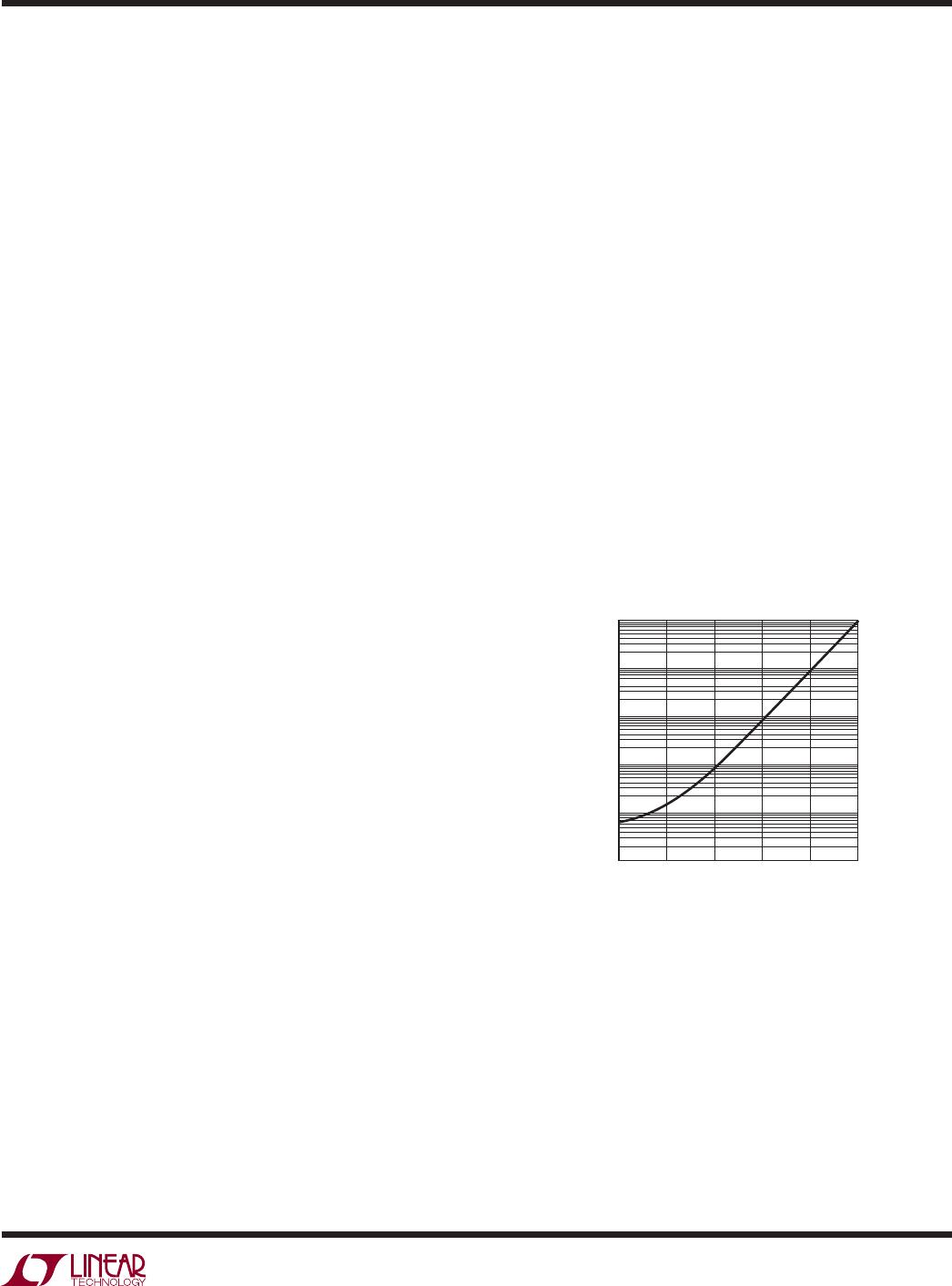
Selecting the Reset Timing Capacitor
The reset timeout period for LTC2905 is adjustable in order
to accommodate a variety of microprocessor applications.
Connecting a capacitor, C
TMR
, between the TMR pin and
ground sets the reset timeout period, t
RST
. The following
formula determines the value of capacitor needed for a
particular reset timeout period:
C
TMR
= t
RST
• 110 • 10
–9
[F/s]
For example, using a standard capacitor value of 22nF
would give a 22000/110 = 200ms delay.
Figure 1 shows the desired delay time as a function of the
value of the timer capacitor that should be used:
Leaving the TMR pin open with no external capacitor gen-
erates a reset timeout of approximately 200μs. For long
reset timeout, the only limitation is the availability of large
value capacitor with low leakage. The TMR capacitor will
never charge if the leakage current exceeds the minimum
TMR charging current of 2.1μA (typical).
Figure 1. Reset Timeout Period vs Capacitance
C
TMR
(FARAD)
10p 100p 1n 10n 100n
RESET TIME OUT PERIOD, t
RST
(ms)
29045 F01
10000
1000
100
10
1
0.1
LTC2904/LTC2905
12
29045fd
APPLICATIONS INFORMATION
Output Rise and Fall Time Estimation
The RST and RST outputs have strong pull-down capabil-
ity. The following formula estimates the output fall time
(90% to 10%) for a particular external load capacitance
(C
LOAD
):
t
FALL
≈ 2.2 • R
PD
• C
LOAD
where R
PD
is the on-resistance of the internal pull-down
transistor estimated to be typically 40Ω at room tempera-
ture (25°C) and C
LOAD
is the external load capacitance on
the pin. Assuming a 150pF load capacitance, the fall time
is about 13ns.
The rise time, on the RST and RST pins is limited by weak
internal pull-up current sources to V
CC
. The following
formula estimates the output rise time (10% to 90%) at
the RST and RST pins:
t
RISE
≈ 2.2 R
PU
• C
LOAD
where R
PU
is the on-resistance of the pull-up transistor.
Notice that this pull-up transistor is modeled as a
6μA current source in the Block Diagram as a typical
representation.
The on-resistance as a function of the V
CC
= Max (V1, V2)
voltage (for V
CC
> 1V) at room temperature is estimated
as follows:
R
MAX V V V
PU
610
12 1
5
(,)
At V
CC
= 3.3V, R
PU
is about 260k. Using 150pF for load
capacitance, the rise time is 86μs. An external pull-up
resistor may be used if the output needs to pull up faster
and/or to a higher voltage, for example: the rise time re-
duces to 3.3μs for a 150pF load capacitance, when using
a 10k pull-up resistor.
RST and RST Output Characteristics
The DC characteristics of the RST and RST pull-up and
pull-down strength are shown in the Typical Performance
Characteristics section. Both RST and RST have a weak
internal pull-up to V
CC
= Max (V1, V2) and a strong pull-
down to ground.
The weak pull-up and strong pull-down arrangement allow
these two pins to have open-drain behavior while possess-
ing several other benefi cial characteristics.
The weak pull-ups eliminate the need for external pull-up
resistors when the rise time on these pins is not critical. On
the other hand, the open-drain RST confi guration allows
for wired-OR connections and can be useful when more
than one signal needs to pull down on the RST line.
As noted in the Power-Up and Power-Down sections the
circuits that drive RST and RST are powered by V
CC
. During
fault condition, V
CC
of at least 1V guarantees a maximum
V
OL
= 0.4V at RST. However, at V
CC
= 1V the weak pull-up
current on RST is barely turned on. Therefore, an external
pull-up resistor of no more than 100k is recommended on
the RST pin if the state and pull-up strength of the RST
pin is crucial at very low V
CC
.
Note however, by adding an external pull-up resistor, the
pull-up strength on the RST pin is increased. Therefore,
if it is connected in a wired-OR connection, the pull-down
strength of any single device needs to accommodate this
additional pull-up strength.

LTC2905ITS8#TRMPBF

Mfr. #:
Manufacturer:
Analog Devices Inc.
Description:
Supervisory Circuits Prec 2x S Mon w/ Pin-Sel Thresholds
Lifecycle:
New from this manufacturer.
Delivery:
DHL FedEx Ups TNT EMS
Payment:
T/T Paypal Visa MoneyGram Western Union