LTC2904/LTC2905
4
29045fd
TYPICAL PERFORMANCE CHARACTERISTICS
TEMPERATURE (oC)
THRESHOLD VOLTAGE, V
RT50
(V)
29045 G01
4.75
4.70
4.65
4.60
4.55
4.50
4.45
4.40
4.35
–50 100
25
75
–25
0
50
5%
7.5%
10%
TEMPERATURE (oC)
THRESHOLD VOLTAGE, V
RT33
(V)
3.120
3.070
3.020
2.970
2.920
2.870
29045 G02
–50 100
25
75
–25
0
50
5%
7.5%
10%
TEMPERATURE (oC)
THRESHOLD VOLTAGE, V
RT25
(V)
29045 G03
2.375
2.325
2.275
2.225
2.175
–50 100
25
75
–25
0
50
5%
7.5%
10%
TEMPERATURE (oC)
THRESHOLD VOLTAGE, V
RT18
(V)
29045 G04
1.705
1.685
1.665
1.645
1.625
1.605
1.585
1.565
–50 100
25
75
–25
0
50
5%
7.5%
10%
TEMPERATURE (oC)
THRESHOLD VOLTAGE, V
RT15
(V)
29045 G05
1.425
1.405
1.385
1.365
1.345
1.325
1.305
–50 100
25
75
–25
0
50
5%
7.5%
10%
TEMPERATURE (oC)
THRESHOLD VOLTAGE, V
RT12
(V)
1.135
1.125
1.115
1.105
1.095
1.085
1.075
1.065
1.055
1.045
29045 G06
–50 100
25
75
–25
0
50
5%
7.5%
10%
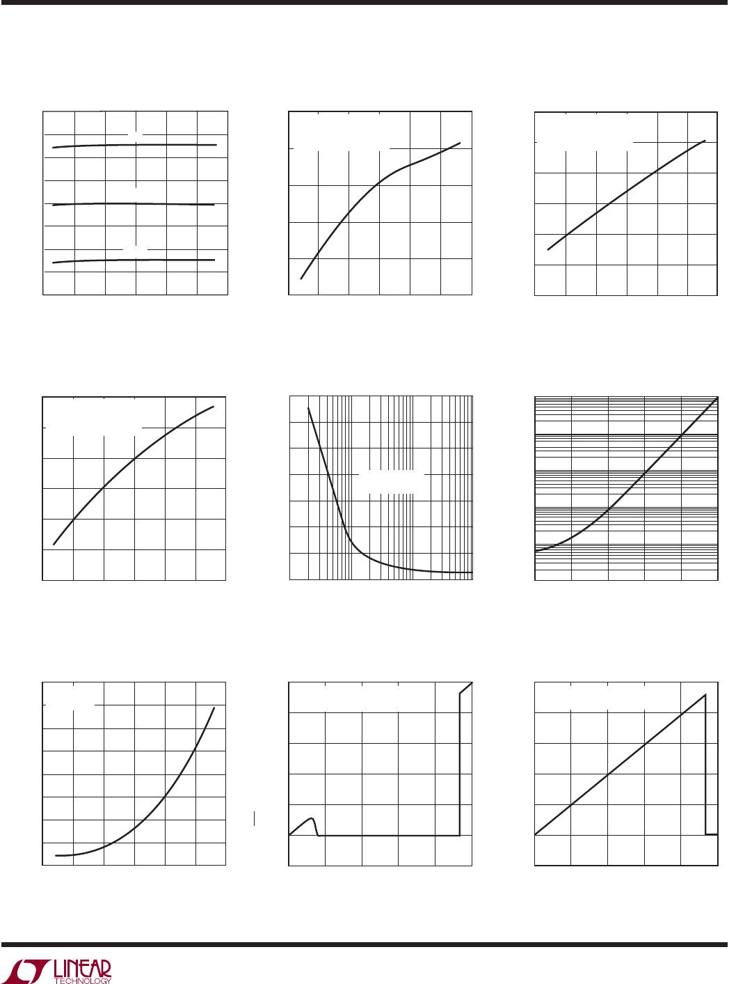
1.8V Threshold Voltage
vs Temperature
1.5V Threshold Voltage
vs Temperature
1.2V Threshold Voltage
vs Temperature
5V Threshold Voltage
vs Temperature
3.3V Threshold Voltage
vs Temperature
2.5V Threshold Voltage
vs Temperature
Specifi cations are at T
A
= 25°C unless otherwise noted.
Note 1: Stresses beyond those listed under Absolute Maximum Ratings
may cause permanent damage to the device. Exposure to any Absolute
Maximum Rating condition for extended periods may affect device
reliability and lifetime.
Note 2: The greater of V1, V2 is the internal supply voltage (V
CC
).
Note 3: All currents into pins are positive; all voltages are referenced to
GND unless otherwise noted.
Note 4: For reset thresholds test conditions refer to the voltage threshold
programming table in the Applications Information section.
Note 5: The output pins RST and RST have an internal pull-up to V
CC
of
typically –6μA. However, an external pull-up resistor may be used when
faster rise time is required or for V
OH
voltages greater than V
CC
.
Note 6: The input current to the three-state input pins are the pull-up
and the pull-down current when the pins are either set to V1 or GND
respectively. In the open state, the maximum leakage current to V1 or GND
permissible is 10μA.
ELECTRICAL CHARACTERISTICS
LTC2904/LTC2905
5
29045fd
TEMPERATURE (oC)
THRESHOLD VOLTAGE, V
RT10
(V)
29045 G07
0.950
0.940
0.930
0.920
0.910
0.900
0.890
0.880
0.870
–50 100
25
75
–25
0
50
5%
7.5%
10%
TEMPERATURE (oC)
I
V1
(MA)
21.5
21.0
20.5
20.0
19.5
19.0
29045 G08
–50 100
25
75
–25
0
50
V1 = 5V
V2 = 3.3V
S1
=
S2
= TOL = 1.4V
TEMPERATURE (oC)
I
V2
(MA)
29045 G09
1.8
1.7
1.6
1.5
1.4
1.3
1.2
–50 100
25
75
–25
0
50
V1 = 5V
V2 = 3.3V
S1
=
S2
= TOL = 1.4V
TYPICAL PERFORMANCE CHARACTERISTICS
TEMPERATURE (oC)
I
V2
(MA)
29045 G10
20.0
19.5
19.0
18.5
18.0
17.5
17.0
–50 100
25
75
–25
0
50
V1 = 2.5V
V2 = 3.3V
S1 = S2 = TOL = 1.4V
COMPARATOR OVERDRIVE VOLTAGE (% OF V
RTX
)
0.1
TYPICAL TRANSIENT DURATION (Ms)
700
600
500
400
300
200
100
0
1 10 100
29045 G11
RESET OCCURS
ABOVE CURVE
C
TMR
(FARAD)
10p 100p 1n 10n 100n 1M
RESET TIME OUT PERIOD, t
RST
(ms)
29045 G12
10000
1000
100
10
1
0.1
TEMPERATURE (oC)
RESET TIME-OUT PERIOD, t
RST
(ms)
29045 G13
235
230
225
220
215
210
205
200
195
–50 100
25
75
–25
0
50
CRT = 22nF
(FILM)
V1 (V)
0
RST OUTPUT VOLTAGE (V)
5
4
3
2
1
0
–1
1234
29045 G14
5
V2 = S1 = S2 = TOL = V1
10k PULL-UP RESISTOR
V1 (V)
0
RST OUTPUT VOLTAGE (V)
5
4
3
2
1
0
–1
1234
29045 G15
5
V2 = S1 = S2 = TOL = V1
10k PULL-UP RESISTOR
Reset Timeout Period (t
RST
)
vs Temperature RST Output Voltage vs V1 RST Output Voltage vs V1
I
V2
vs Temperature
Typical Transient Duration
vs Comparator Overdrive (V1, V2)
Reset Time Out Period (t
RST
)
vs Capacitance (C
TMR
)
1V Threshold Voltage
vs Temperature I
V1
vs Temperature I
V2
vs Temperature
Specifi cations are at T
A
= 25°C unless otherwise noted.
LTC2904/LTC2905
6
29045fd
RST PULL-DOWN CURRENT, I
RST
(mA)
0
RST OUTPUT VOLTAGE LOW, V
OL
(V)
20
1.8
1.6
1.4
1.2
1.0
0.8
0.6
0.4
0.2
0
29045 G19
10 50 604030
25oC
85oC
–40oC
V1 = 5V
V2 = 3V
S1 = S2 = TOL = V1
NO PULL-UP R
RST PULL-DOWN CURRENT, I
RST
(mA)
0
RST OUTPUT VOLTAGE LOW, V
OL
(V)
20
1.8
1.6
1.4
1.2
1.0
0.8
0.6
0.4
0.2
0
29045 G20
10 50 604030
25oC
85oC
–40oC
V1 = 5V
V2 = 3.3V
S1 = S2 = TOL = V1
NO PULL-UP R
SUPPLY VOLTAGE, V
CC
(V)
2.0
RST PULL-UP CURRENT, I
RST
(MA)
4.0
–18
–16
–14
–12
–10
–8
–6
–4
–2
0
29045 G21
3.0 5.0
2.5
4.5
3.5
V
RT25
V
RT33
V
RT50
TOL = GND
SUPPLY VOLTAGE, V
CC
(V)
2.0
4.0
29045 G22
3.0 5.0
2.5
4.5
3.5
RST PULL-UP CURRENT, I
RST
(MA)
–16
–14
–12
–10
–8
–6
–4
–2
0
TOL = V1
V
RT25
V
RT33
V
RT50
OUTPUT SOURCE CURRENT, I
RST
(MA)
–12
RST OUTPUT VOLTAGE HIGH, V
OH
(V)
3.0
2.5
2.0
1.5
1.0
0.5
–10
–8 –6 –4
29045 G23
–2 0
V1 = 3.3V
V2 = 1.8V
S1 = TOL =V1
S2 = OPEN
NO PULL-UP R
25oC
85oC
–40oC
OUTPUT SOURCE CURRENT, I
RST
(MA)
–7
RST OUTPUT VOLTAGE HIGH, V
OH
(V)
3.5
3.0
2.5
2.0
1.5
1.0
0.5
–1
–8 –6 –3–4–5
29045 G24
–2 0
V1 = 3.3V
V2 = 1.5V
S1 = TOL = V1
S2 = OPEN
NO PULL-UP R
25oC
85oC
–40oC
RST Pull-Up Current (I
RST
)
vs Supply Voltage (V
CC
)
RST Output Voltage High (V
OH
)
vs RST Output Source Current (I
RST
)
RST Output Voltage High (V
OH
)
vs RST Output Source Current (I
RST
)
RST Output Voltage Low (V
OL
)
vs RST Pull-Down Current (I
RST
)
RST Output Voltage Low (V
OL
)
vs RST Pull-Down Current (I
RST
)
RST Pull-Up Current (I
RST
)
vs Supply Voltage (V
CC
)
TYPICAL PERFORMANCE CHARACTERISTICS
Specifi cations are at T
A
= 25°C unless otherwise noted.
V1 (V)
0
RST OUTPUT VOLTAGE (V)
5
4
3
2
1
0
–1
1234
29045 G16
5
V2 = S1 = S2 = TOL = V1
10pF CAPACITOR AT RST
SUPPLY VOLTAGE, V
CC
(V)
0
RST PULL-DOWN CURRENT, I
RST
(mA)
5
4
3
2
1
0
4
29045 G17
123 5
RST AT 150mV
RST AT 50mV
V2 = S1 = S2 = TOL = V1
NO PULL-UP R
SUPPLY VOLTAGE, V
CC
(V)
0
RST PULL-DOWN CURRENT, I
RST
(mA)
5
4
3
2
1
0
4
29045 G18
123 5
RST AT 150mV
RST AT 50mV
S1
= V2 = V1
TOL = S2 = GND
NO PULL-UP R
RST Output Voltage vs V1
RST Pull-Down Current (I
RST
)
vs Supply Voltage (V
CC
)
RST Pull-Down Current (I
RST
)
vs Supply Voltage (V
CC
)

LTC2905ITS8#TRMPBF

Mfr. #:
Manufacturer:
Analog Devices Inc.
Description:
Supervisory Circuits Prec 2x S Mon w/ Pin-Sel Thresholds
Lifecycle:
New from this manufacturer.
Delivery:
DHL FedEx Ups TNT EMS
Payment:
T/T Paypal Visa MoneyGram Western Union