ACPL-W456-020E

10
Figure 17. AC Equivalent Circuit for Figure 12 during Common Mode Tran-
sients.
Figure 16. AC Equivalent Circuit for Figure 15 during Common Mode Tran-
sients.
C
LEDN
V
CM
I
TOTAL
*
20 kΩ
100 pF
V
OUT
61
52
43
SHIELD
+
-
* THE ARROWS INDICATE THE DIRECTION
OF CURRENT FLOW DURING + dV
CM
/dt
300 Ω
I
F
I
CLEDP
C
LED01
I
CLED01
SHIELD
I
CLEDN
*
C
LEDN
V
CM
+ V
R
** -
20 kΩ
100 pF
V
OUT
61
52
43
SHIELD
+
-
* THE ARROWS INDICATE THE DIRECTION OF CURRENT
FLOW FOR + dV
CM
/dt TRANSIENTS.
** OPTIONAL CLAMPING DIODE FOR IMPROVED CMH
PERFORMANCE. V
R
< V
F (OFF)
DURING + dV
CM
/dt
300 Ω
C
LEDP
C
LED01
-
pF
CMR With The LED O (CMR
H
)
A high CMR LED drive circuit must keep the LED o (V
F
≤ V
F(OFF)
) during common mode transients. For example,
during a +dV
CM
/dt transient in Figure 17, the current
owing through C
LEDN
is supplied by the parallel com-
bination of the LED and series resistor. As long as the
voltage developed across the resistor is less than V
F(OFF)
the LED will remain o and no common mode failure
will occur. Even if the LED momentarily turns on, the
100 pF capacitor from pins 5-4 will keep the output from
dipping below the threshold. The recommended LED
drive circuit (Figure 12) provides about 10 V of margin
between the lowest optocoupler output voltage and a
3 V IPM threshold during a 15kV/µs transient with V
CM
= 1500 V. Additional margin can be obtained by adding
a diode in parallel with the resistor, as shown by the
dashed line connection in Figure 17, to clamp the voltage
across the LED below V
F(OFF)
.
Since the open collector drive circuit, shown in Figure 18,
cannot keep the LED o during a +dV
CM
/dt transient, it is
not desirable for applications requiring ultra high CMR
H
performance. Figure 19 is the AC equivalent circuit for
Figure 18 during common mode transients. Essentially
all the current  owing through C
LEDN
during a +dV
CM
/dt
transient must be supplied by the LED. CMR
H
failures can
occur at dv/dt rates where the current through the LED
and C
LEDN
exceeds the input threshold. Figure 20 is an al-
ternative drive circuit which does achieve ultra high CMR
performance by shunting the LED in the o state.
Figure 20. Recommended LED Drive Circuit for Ultra High CMR.
Figure 19. AC Equivalent Circuit for Figure 18 during Common Mode Tran-
sients.
Figure 18. Not Recommended Open Collector LED Drive Circuit.
+5 V
Q1
61
52
43
SHIELD
Q1
I
CLEDN
*
C
LEDN
V
CM
20 kΩ
100 pF
V
OUT
61
52
43
SHIELD
+
-
* THE ARROWS INDICATE THE DIRECTION OF CURRENT
FLOW FOR + dV
CM
/dt
TRANSIENTS.
300 Ω
C
LEDP
C
LED01
Q1
+
-
C
LEDP
+5 V
61
52
43
SHIELD
11
IPM Dead Time and Propagation Delay Speci cations
The ACPL-P456/W456 includes a Propagation Delay
Di erence speci cation intended to help designers
minimize dead time” in their power inverter designs.
Dead time is the time period during which both the high
and low side power transistors (Q1 and Q2 in Figure 21)
are o . Any overlap in Q1 and Q2 conduction will result
in large currents  owing through the power devices
between the high and low voltage motor rails.
To minimize dead time the designer must consider
the propagation delay characteristics of the optocou-
pler as well as the characteristics of the IPM IGBT gate
drive circuit. Considering only the delay characteristics
of the optocoupler (the characteristics of the IPM IGBT
gate drive circuit can be analyzed in the same way) it is
important to know the minimum and maximum turn on
(t
PHL
) and turn-o (t
PLH
) propagation delay speci cations,
preferably over the desired operating temperature range.
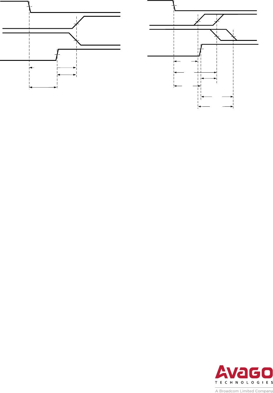
The limiting case of zero dead time occurs when the input
to Q1 turns o at the same time that the input to Q2 turns
on. This case determines the minimum delay between
LED1 turn-o and LED2 turn-on, which is related to the
worst case optocoupler propagation delay waveforms,
as shown in Figure 22. A minimum dead time of zero is
achieved in Figure 22 when the signal to turn on LED2
is delayed by (t
PLH
max - t
PHL
min) from the LED1 turn
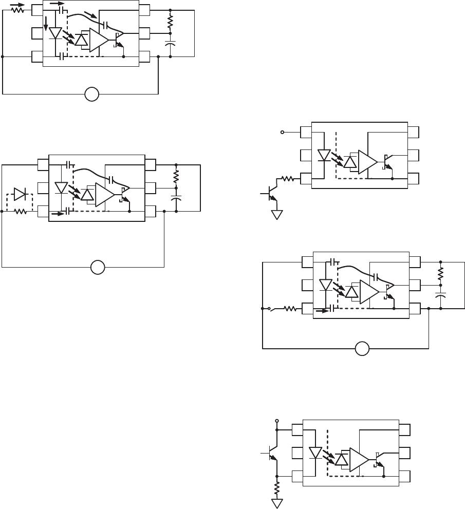
Figure 21. Typical Application Circuit.
o . Note that the propagation delays used to calculate
PDD are taken at equal temperatures since the optocou-
plers under consideration are typically mounted in close
proximity to each other. (Speci cally, previous equation
are not the same as the t
PLH
max and t
PHL
min, over the
full operating temperature range, speci ed in the data
sheet.) This delay is the maximum value for the propaga-
tion delay di erence speci cation which is speci ed at
450 ns for the ACPL-P456/W456 over an operating tem-
perature range of -40°C to 100°C.
Delaying the LED signal by the maximum propagation
delay di erence ensures that the minimum dead time is
zero, but it does not tell a designer what the maximum
dead time will be. The maximum dead time occurs in
the highly unlikely case where one optocoupler with
the fastest t
PLH
and another with the slowest t
PHL
are in
the same inverter leg. The maximum dead time in this
case becomes the sum of the spread in the t
PLH
and t
PHL
propagation delays as shown in Figure 23. The maximum
dead time is also equivalent to the di erence between
the maximum and minimum propagation delay di er-
ence speci cations. The maximum dead time (due to the
optocouplers) for the ACPL-P456/W456 are 600 ns (= 450
ns - (-150 ns)) over an operating temperature range of -
40°C to 100°C.
M
IPM
+HV
-HV
310 Ω
+5 V
CMOS
0.1 μF
V
CC1
20 kΩ
V
OUT1
61
52
43
SHIELD
I
LED1
310 Ω
+5 V
CMOS
0.1 μF
V
CC2
20 kΩ
V
OUT2
61
52
43
SHIELD
I
LED2
ACPL-P/W456
ACPL-P/W456
ACPL-P/W456
ACPL-P/W456
ACPL-P/W456
MM
-
+5 V
1
2
3
I
LED1
+5 V
3
Figure 22. Minimum LED Skew for Zero Dead Time.
Figure 23. Waveforms for Deadtime Calculation.
V
OUT1
V
OUT2
I
LED2
t
PLH
MIN.
MAXIMUM DEAD TIME (DUE TO OPTOCOUPLER)
= (t
PLH MAX. -
t
PLH MIN.
)
+
(t
PHL MAX. -
t
PHL MIN.
)
= (t
PLH MAX. -
t
PHL MIN.
) -
(t
PLH MIN. -
t
PHL MAX.
)
= PDD* MAX. - PDD* MIN.
t
PHL
MIN.
I
LED1
Q1 ON
Q2 OFF
Q1 OFF
Q2 ON
*PDD = PROPAGATION DELAY DIFFERENCE
t
PLH
MAX.
t
PHL
MAX.
PDD*
MAX.
MAX.
DEAD TIME
NOTE: THE PROPAGATION DELAYS USED TO CALCULATE THE MAXIMUM
DEAD TIME ARE TAKEN AT EQUAL TEMPERATURES.
V
OUT1
V
OUT2
I
LED2
t
PLH MAX.
PDD* MAX. =
(t
PLH-
t
PHL
)
MAX. =
t
PLH MAX. -
t
PHL MIN.
t
PHL
MIN.
I
LED1
Q1 ON
Q2 OFF
Q1 OFF
Q2 ON
*PDD = PROPAGATION DELAY DIFFERENCE
NOTE: THE PROPAGATION DELAYS USED TO CALCULATE
PDD ARE TAKEN AT EQUAL TEMPERATURES.
For product information and a complete list of distributors, please go to our web site: www.avagotech.com
Avago, Avago Technologies, and the A logo are trademarks of Avago Technologies in the United States and other countries.
Data subject to change. Copyright © 2005-2016 Avago Technologies. All rights reserved.
AV02-1306EN - August 12, 2016

ACPL-W456-020E

Mfr. #:
Manufacturer:
Broadcom / Avago
Description:
Logic Output Optocouplers 1MBd 3750Vrms
Lifecycle:
New from this manufacturer.
Delivery:
DHL FedEx Ups TNT EMS
Payment:
T/T Paypal Visa MoneyGram Western Union