9
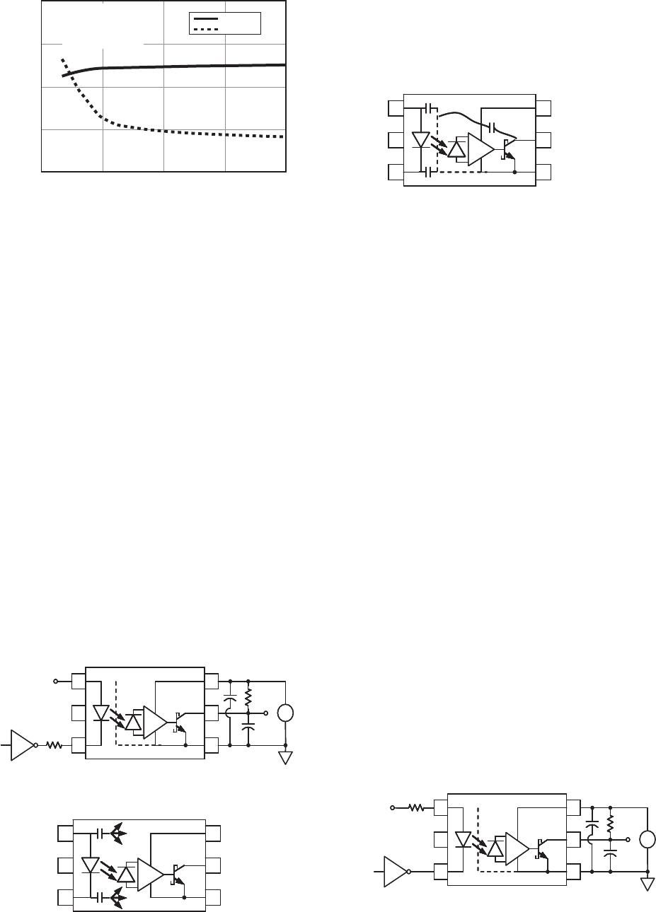
Figure 14. Optocoupler Input to Output Capacitance Model for Shielded
Optocouplers.
Another cause of CMR failure for a shielded optocoupler
is direct coupling to the optocoupler output pins through
C
LEDO1
in Figure 14. Many factors in uence the e ect and
magnitude of the direct coupling including: the position
of the LED current setting resistor and the value of the
capacitor at the optocoupler output (C
L
).
Figure 13. Optocoupler Input to Output Capacitance Model for Unshielded
Optocouplers.
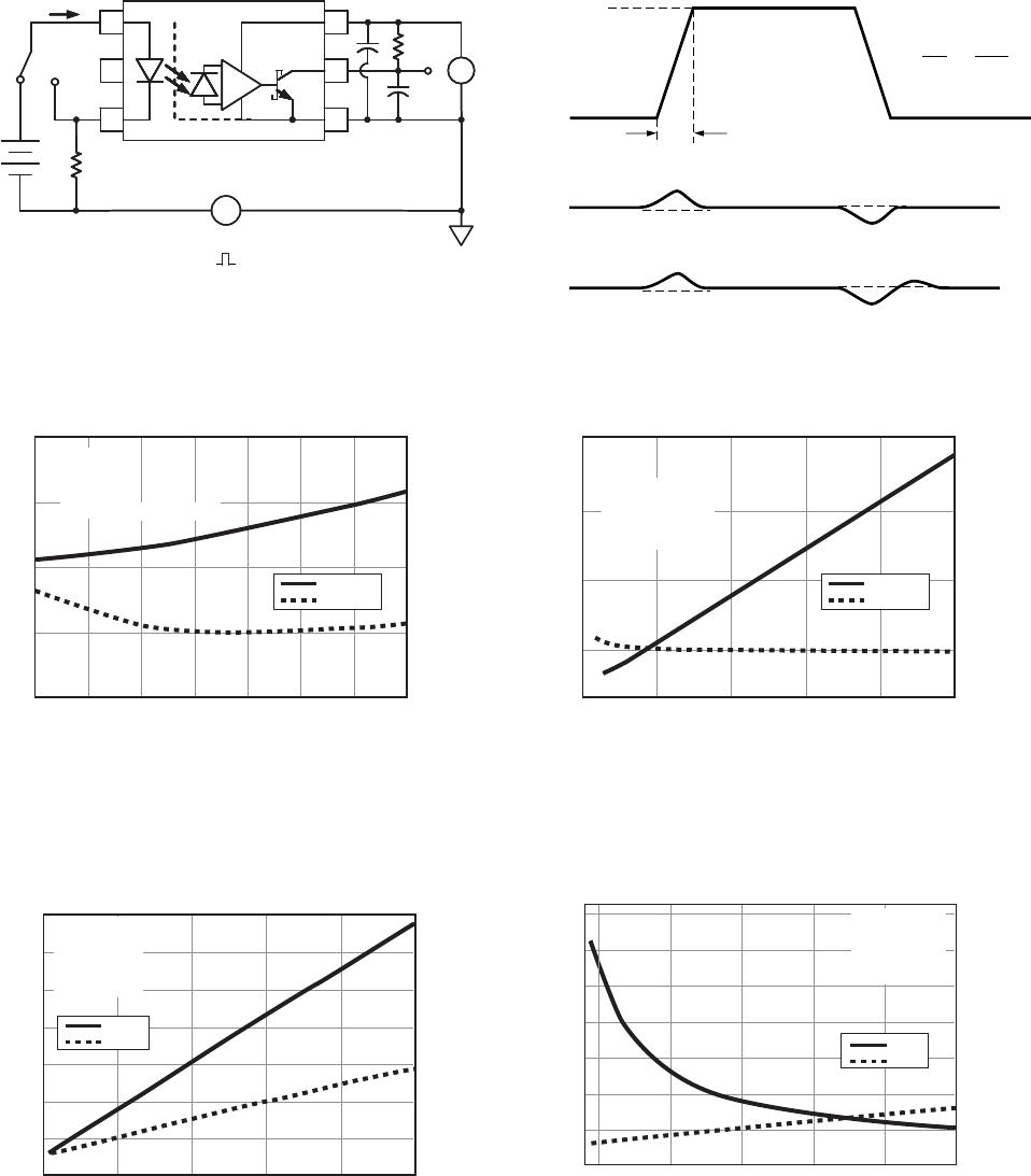
Figure 12. Recommended LED Drive Circuit.
Applications Information
LED Drive Circuit Considerations For Ultra High CMR
Performance
Without a detector shield, the dominant cause of opto-
coupler CMR failure is capacitive coupling from the input
side of the optocoupler, through the package, to the
detector IC as shown in Figure 13. The ACPL-P456/W456
improve CMR performance by using a detector IC with
an optically transparent Faraday shield, which diverts the
capacitively coupled current away from the sensitive IC
circuitry. However, this shield does not eliminate the ca-
pacitive coupling between the LED and the optocoupler
output pin and output ground as shown in Figure 14.
This capacitive coupling causes perturbations in the LED
current during common mode transients and becomes
the major source of CMR failures for a shielded optocou-
pler. The main design objective of a high CMR LED drive
circuit becomes keeping the LED in the proper state (on
or o ) during common mode transients. For example,
the recommended application circuit (Figure 12), can
achieve 15 kV/µs CMR while minimizing component
complexity. Note that a CMOS gate is recommended in
Figure 12 to keep the LED o when the gate is in the high
state.
Figure 11. Propagation Delay vs. Input Current.
t
P
– PROPAGATION DELAY – ns
100
I
F
– FORWARD LED CURRENT – mA
300
10
500
15
V
CC
= 15 V
200
400
t
PLH
5020
t
PHL
C
L
= 100 pF
R
L
= 20 kΩ
T
A
= 25 C
CAPACITANCE
310 Ω
+5 V
CMOS
0.1 μF
+
-
V
CC
= 15 V
20 kΩ
C
L
*
V
OUT
61
52
43
SHIELD
* 100 pF TOTAL
+
-
61
52
43
C
LEDP
C
LEDN
61
52
43
SHIELD
C
LEDP
C
LEDN
C
LED01
CMR With The LED On (CMR
L
)
A high CMR LED drive circuit must keep the LED on
during common mode transients. This is achieved by
overdriving the LED current beyond the input threshold
so that it is not pulled below the threshold during a
transient. The recommended minimum LED current of 10
mA provides adequate margin over the maximum I
TH
of
4.0 mA (see Figure 1) to achieve 15 kV/µs CMR.
The placement of the LED current setting resistor e ects
the ability of the drive circuit to keep the LED on during
transients and interacts with the direct coupling to the
optocoupler output. For example, the LED resistor in
Figure 15 is connected to the anode. Figure 16 shows
the AC equivalent circuit for Figure 15 during common
mode transients. During a +dV
CM
/dt in Figure 16, the
current available at the LED anode (Itotal) is limited by
the series resistor. The LED current (I
F
) is reduced from its
DC value by an amount equal to the current that ows
through C
LEDP
and C
LEDO1
. The situation is made worse
because the current through C
LEDO1
has the e ect of
trying to pull the output high (toward a CMR failure) at
the same time the LED current is being reduced. For this
reason, the recommended LED drive circuit (Figure 12)
places the current setting resistor in series with the LED
cathode. Figure 17 is the AC equivalent circuit for Figure
12 during common mode transients. In this case, the
LED current is not reduced during a +dV
CM
/dt transient
because the current owing through the package capaci-
tance is supplied by the power supply. During a -dV
CM
/
dt transient, however, the LED current is reduced by the
amount of current owing through C
LEDN
. But, better
CMR performance is achieved since the current owing
in C
LEDO1
during a negative transient acts to keep the
output low.
Figure 15. LED Drive Circuit with Resistor Connected to LED Anode (Not
Recommended).
* 100 pF TOTAL
CAPACITANCE
310 Ω
+5 V
CMOS
0.1 μF
+
-
V
CC
= 15 V
20 kΩ
C
L
*
V
OUT
61
52
43
SHIELD
+5 V