Expand menu
Hello, Sign in
My Account
0
Cart
Home
Products
Sensors
Semiconductors
Passive Components
Connectors
Power
Electromechanical
Optoelectronics
Circuit Protection
Integrated Circuits - ICs
Main Products
Manufacturers
Blog
Services
About OMO
About Us
Contact Us
Check Stock
NCV8406ADTRKG
P1-P3
P4-P6
P7-P9
P10-P12
NCV8406, NCV8406A
www
.onsemi.com
4
TYPICAL PERFORMANCE CUR
VES
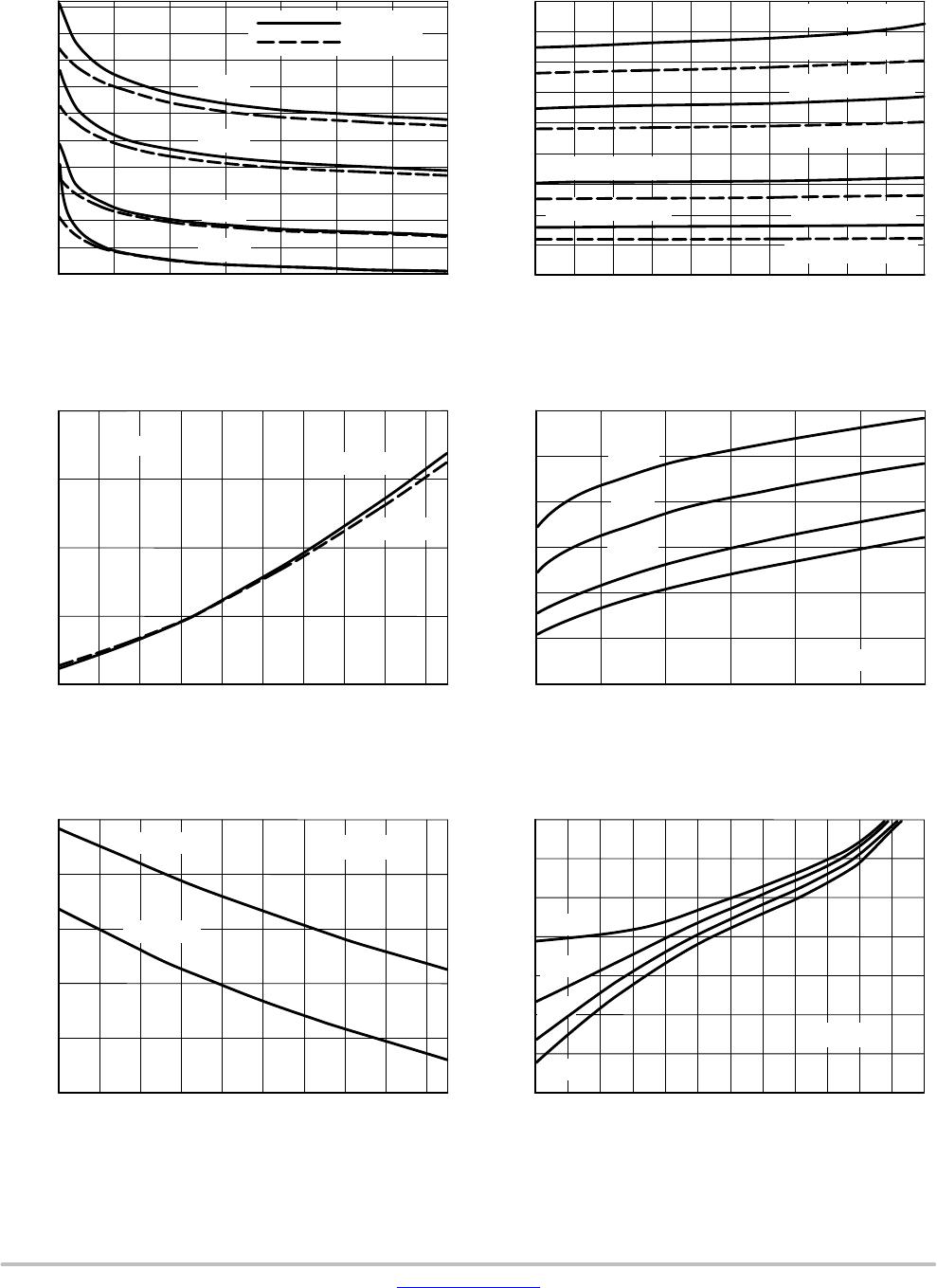
Figure 2. Single Pulse Maximum Switch−off
Current vs. Load Inductance
Figure 3. Single−Pulse Maximum Switching
Energy vs. Load Inductance
L (mH)
L (mH)
100
10
1
10
100
10
100
1000
Figure 4. Single Pulse Maximum Inductive
Switch−off Current vs. Time in Clamp
Figure 5. Single−Pulse Maximum Inductive
Switching Energy vs. Time in Clamp
TIME IN CLAMP (ms)
TIME IN CLAMP (ms)
10
1
0.1
1
10
10
1
10
1000
ILmax (A)
Emax (mJ)
ILmax (A)
Emax (mJ)
T
Jstart
= 25
°
C
T
Jstart
= 150
°
C
T
Jstart
= 25
°
C
T
Jstart
= 150
°
C
T
Jstart
= 25
°
C
T
Jstart
= 150
°
C
T
Jstart
= 25
°
C
T
Jstart
= 150
°
C
10
100
3 V
150
°
C
V
DS
(V)
V
GS
(V)
15
10
5
0
0
2
6
10
12
5
4
3
2
1
0
0
3
6
9
12
I
D
(A)
I
D
(A)
8
V
GS
= 2.5 V
3.3 V
4 V
5 V
6 V
7 V
8 V
9 V
10 V
−40
°
C
25
°
C
100
°
C
Figure 6. On−state Output Characteristics
Figure 7. T
ransfer Characteristics
T
a
= 25
°
C
V
DS
= 10 V
4
NCV8406, NCV8406A
www
.onsemi.com
5
TYPICAL PERFORMANCE CUR
VES
Figure 8. R
DS(on)
vs. Gate−Source V
oltage
Figure 9. R
DS(on)
vs. Drain Current
V
GS
(V)
I
D
(A)
R
DS(on)
(m
W
)
R
DS(on)
(m
W
)
−40
°
C
25
°
C
100
°
C
150
°
C
−40
°
C, V
GS
= 5 V
−40
°
C, V
GS
= 10 V
25
°
C, V
GS
= 5 V
25
°
C, V
GS
= 10 V
100
°
C, V
GS
= 5 V
100
°
C, V
GS
= 10 V
150
°
C, V
GS
= 5 V
Figure 10. Normalized R
DS(on)
vs. T
emperature
Figure 1
1. Current Limit vs. Gate−Source
V
oltage
T (
°
C)
V
GS
(V)
120
100
80
40
20
0
−20
−40
0.5
1.0
1.5
2.0
2.5
NORMALIZED R
DS(on)
I
LIM
(A)
60
−40
°
C
25
°
C
100
°
C
140
V
GS
= 5 V
V
GS
= 10 V
100
200
300
400
500
600
3456
789
1
0
50
100
200
300
350
400
450
500
0.5
1
1.5
2
2.75
150
°
C, V
GS
= 10 V
3
5
7
11
15
45
6
8
9
1
0
150
°
C
0.75
1.25
1.75
2.25
3
150
I
D
= 2 A
V
DS
= 10 V
150
250
350
450
550
ID = 2 A
ID = 0.5 A
250
2.5
7
9
13
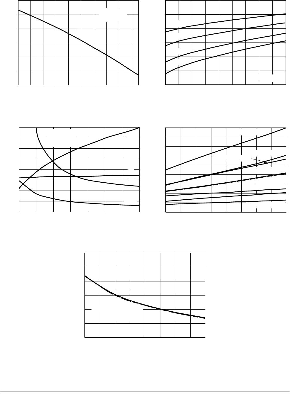
Figure 12. Current Limit vs. Junction
T
emperature
Figure 13. Drain−to−Source Leakage Current
T
J
(
°
C)
V
DS
(V)
70
60
50
40
30
20
10
0.0001
0.01
0.1
1
10
100
1000
I
LIM
(A)
I
DSS
(
m
A)
−40
°
C
25
°
C
100
°
C
150
°
C
5
7
9
11
15
−40
−20
0
20
40
60
80
100
120
140
V
GS
= 5 V
V
GS
= 10 V
V
DS
= 10 V
V
GS
= 0 V
0.001
13
NCV8406, NCV8406A
www
.onsemi.com
6
TYPICAL PERFORMANCE CUR
VES
Figure 14. Normalized Threshold V
oltage vs.
T
emperature
Figure 15. Source−Drain Diode Forward
Characteristics
T (
°
C)
I
S
(A)
140
100
60
40
20
0
−20
−40
0.6
0.7
0.8
0.9
1.0
1.1
1.2
8
7
6
5
4
3
2
1
500
600
700
800
1000
1
100
NORMALIZED V
GS(th)
(V)
V
SD
(mV)
80
120
9
10
−40
°
C
25
°
C
100
°
C
150
°
C
Figure 16. Resistive Load Switching Time vs.
Gate−Source V
oltage
V
GS
(V)
10
9
8
7
6
5
4
3
0
200
600
1000
1600
TIME (ns)
t
d(off)
t
d(on)
t
f
t
r
I
D
= 150
m
A
V
DS
= V
GS
1200
V
GS
= 0 V
V
DD
= 13.8 V
I
D
= 2 A
R
G
= 0
W
900
400
800
1400
Figure 17. Resistive Load Switching Time vs.
Gate Resistance
R
G
(
W
)
2000
1500
1000
500
0
−200
200
1400
3000
3400
TIME (ns)
t
d(on)
, V
GS
= 5 V
t
d(off)
, V
GS
= 5 V
t
r
, V
GS
= 5 V
t
f
, V
GS
= 5 V
t
d(on)
, V
GS
= 10 V
t
d(off)
, V
GS
= 10 V
t
r
, V
GS
= 10 V
t
f
, V
GS
= 10 V
2600
2200
1800
1000
600
Figure 18. Drain−Source V
oltage Slope during
T
urn On and T
urn Off vs. Gate Resistance
R
G
(
W
)
2000
1500
1000
500
0
5
10
15
25
35
DRAIN−SOURCE VOL
T
AGE SLOPE (V/
m
s)
20
30
dV
DS
/d
t(off)
, V
GS
= 5 V
dV
DS
/d
t(off)
, V
GS
= 10 V
P1-P3
P4-P6
P7-P9
P10-P12
NCV8406ADTRKG
Mfr. #:
Buy NCV8406ADTRKG
Manufacturer:
ON Semiconductor
Description:
Gate Drivers 65V, SMARTFET
Lifecycle:
New from this manufacturer.
Delivery:
DHL
FedEx
Ups
TNT
EMS
Payment:
T/T
Paypal
Visa
MoneyGram
Western
Union
Products related to this Datasheet
NCV8406ASTT1G
NCV8406ADTRKG
NCV8406ASTT3G
NCV8406STT3G
NCV8406DTRKG