601M-01LFT

DATASHEET
LOW PHASE NOISE CLOCK MULTIPLIER ICS601-01
IDT™ / ICS™
LOW PHASE NOISE CLOCK MULTIPLIER 1
ICS601-01 REV N 051310
Description
The ICS601-01 is a low-cost, low phase noise,
high-performance clock synthesizer for applications
which require low phase noise and low jitter. It is IDT’s
lowest phase noise multiplier, and also the lowest
CMOS part in the industry. Using IDT’s patented
analog and digital Phase-Locked Loop (PLL)
techniques, the chip accepts a 10 - 27 MHz crystal or
clock input, and produces output clocks up to 156 MHz
at 3.3 V.
This product is intended for clock generation. It has low
output jitter (variation in the output period), but input to
output skew and jitter are not defined nor guaranteed.
For applications which require definted input to output
timing, use the ICS670-01.
Features
Packaged in 16-pin SOIC or TSSOP
Pb (lead) free package
Uses fundamental 10 - 27 MHz crystal or clock
Patented PLL with the lowest phase noise
Output clocks up to 156 MHz at 3.3 V
Low phase noise: -132 dBc/Hz at 10 kHz
Low jitter - 18 ps one sigma typ.
Full swing CMOS outputs with 25 mA drive capability
at TTL levels
Advanced, low power, sub-micron CMOS process
Industrial temperature range available
Operating voltage of 3.3V or 5V
Block Diagram
ROM Based
Multipliers
VCO
Divide
X1/ICLK
X2
Crystal or
clock input
Crystal
Oscillator
Reference
Divider
Phase
Comparator
Charge
Pump
Loop
Filter
VCO
S3:0
GND
3
4
VDD
3
CLK
REFOUT
REFEN
OE
ICS601-01
LOW PHASE NOISE CLOCK MULTIPLIER CLOCK MULTIPLIER
IDT™ / ICS™
LOW PHASE NOISE CLOCK MULTIPLIER 2
ICS601-01 REV N 051310
Pin Assignment Multiplier Select Table
0 = connect directly to ground
1 = connect directly to VDD
Pin Descriptions
1
2
3
VDD
4
REFEN
5
6
GND
7
8
GND
REFOUT
S3S1
GND
X2
S2
VDD
16
CLK
VDD
X1/ICLK
S0
OE
15
14
13
12
11
10
9
16 Pin (150 mil) TSSOP or SOIC
S3 S2 S1 S0 CLK (see note 2 on following page)
000 0 TEST
000 1 TEST
0010 Input x1
0011 Input x3
0100 Input x4
0101 Input x5
0110 Input x6
0111 Input x8
100 0 TEST
100 1 Crystal osc. pass through (no PLL)
1010 Input x2
101 1 TEST
1100 Input x8
110 1 Input x10
111 0 Input x12
111 1 Input x16
Pin
Number
Pin
Name
Pin
Type
Pin Description
1 CLK Output Clock output from VCO. Output frequency equals the input frequency times multiplier.
2 REFEN Input Reference clock enable. Turns off the buffered crystal oscillator clock (stops low) when low.
3 VDD Power Connect to +3.3V or +5V. Must match other VDDs.
4 VDD Power Connect to +3.3V or +5V. Must match other VDDs.
5 VDD Power Connect to +3.3V or +5V. Must match other VDDs.
6 X2 XO Crystal connection. Connect to a 10 - 27 MHz fundamental parallel mode crystal.
Leave disconnected for an external clock input.
7 S1 Input Multiplier select pin 1. Determines CLK output per table above. Internal pull-up.
8 X1/ICLK XI Crystal connection. Connect to a 10 - 27 MHz fundamental parallel mode crystal or clock.
9 S2 Input Multiplier select pin 2. Determines CLK output per table above. Internal pull-up.
10 S3 Input Multiplier select pin 3. Determines CLK output per table above. Internal pull-up.
11 S0 Input Multiplier select pin 0. Determines CLK output per table above. Internal pull-up.
12 OE Input Output Enable. Tri-states both output clocks when low. Internal pull-up.
13 REFOUT Output Buffered crystal oscillator clock output. Controlled by REFIN.
14 - 16 GND Power Connect to ground.
ICS601-01
LOW PHASE NOISE CLOCK MULTIPLIER CLOCK MULTIPLIER
IDT™ / ICS™
LOW PHASE NOISE CLOCK MULTIPLIER 3
ICS601-01 REV N 051310
Achieving Low Phase Noise
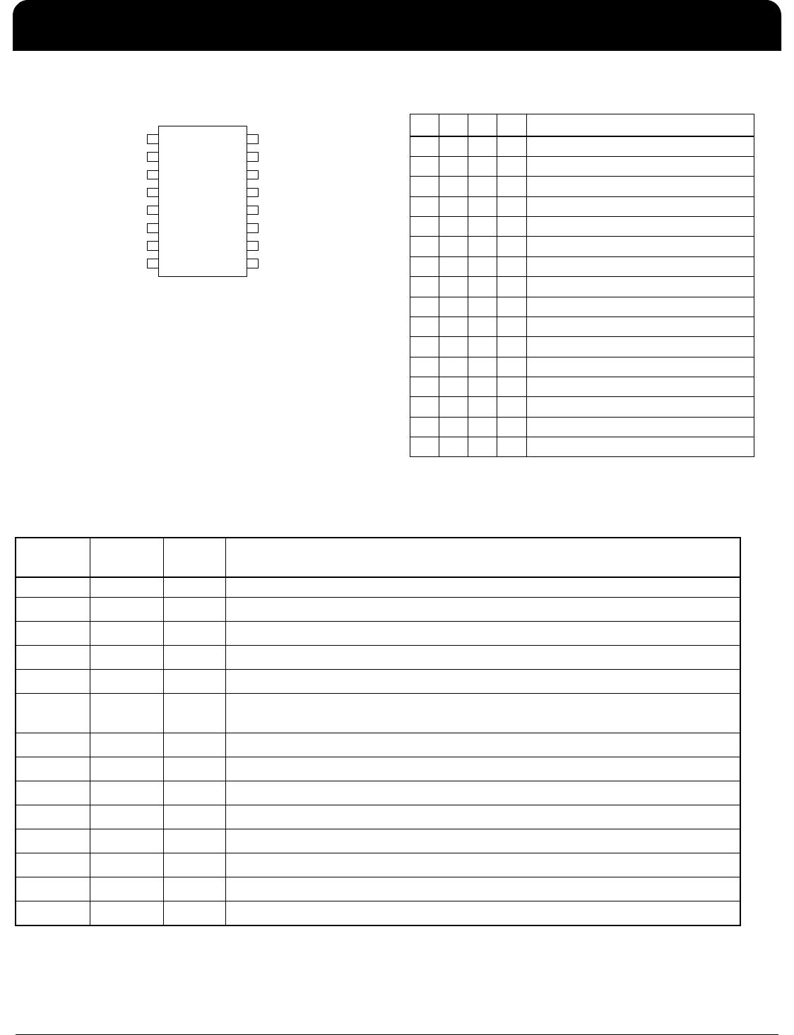
Figure 1 shows a typical phase noise measurement in a 125 MHz system. Therea are a few simple steps that can
be taken to achieve these levels of phase noise from the ICS601-01. Variations in VDD will increase the hase noise,
so it is important to have a stable, low noise supply voltage at the device. Use decoupling capacitors of 0.1µF in
parallel with 0.01µF. It is important to have these capacitors as close as possible to the ICS601-01 supply pins.
Disabling the REFOUT clock is also important for achieving low phase noise; lab tests have shown that this can
reduce the phase noise by as much as 10 dBc/Hz.
External Component/Crystal Selection
The ICS601-01 requires a minimum number of external components for proper operation. Decoupling capacitors of
0.01µF and 0.1µF should be connected between VDD and GND, as close to the part as possible. A series
termination resistor of 33 may be used for each clock output. The crystal must be connected as close to the chip
as possible. The crystal should be fundamental mode, parallel resonant. Do not use third overtone. For exact tuning
when using a crystal, capacitors should beconnected from pins X1 to ground and X2 to ground. In general, the
value of these capacitors is given by the following equation, where CL is the crystal load capacitance: Crystal caps
(pF) = (CL - 5) x 2. So for a crystal with 16 pF load capacitance, two 22 pF caps can be used. For any given board
layout, ICS can measure the board capacitance and recommend the exact capacitance value to use.
Figure 1. Phase Noise of ICS601-01 for 125 MHz output, 25 MHz crystal input.
VDD = 3.3 V, REFOUT disabled.
-140
-120
-100
-80
-60
-40
-20
0
1. 00E+01 1. 00E+02 1. 00E+03 1. 00E+04 1.00E+05 1. 00E+06 1. 00E+07
Offset from Carrier (Hz)
Phase Noise
(
dBc/Hz
)

601M-01LFT

Mfr. #:
Manufacturer:
IDT
Description:
Clock Generators & Support Products LOW PHASE NOISE CLOCK MULTIPLIER
Lifecycle:
New from this manufacturer.
Delivery:
DHL FedEx Ups TNT EMS
Payment:
T/T Paypal Visa MoneyGram Western Union