TC7WH04FU/FK
2009-09-25
1
TOSHIBA CMOS Digital Integrated Circuit Silicon Monolithic
TC7WH04FU,TC7WH04FK
Triple Inverter
Features
• High speed: t
pd
= 3.8ns (typ.) at V
CC
= 5V, C
L
= 15pF
• Low power dissipation: I
CC
= 2μA (max) at Ta = 25°C
• High noise immunity: V
NIH
= V
NIL
= 28% V
CC
(min)
• 5.5-V Tolerant inputs.
• Wide operating voltage range: V
CC
= 2 to 5.5V
• Identical pin assignment and function with TC7W04
Marking
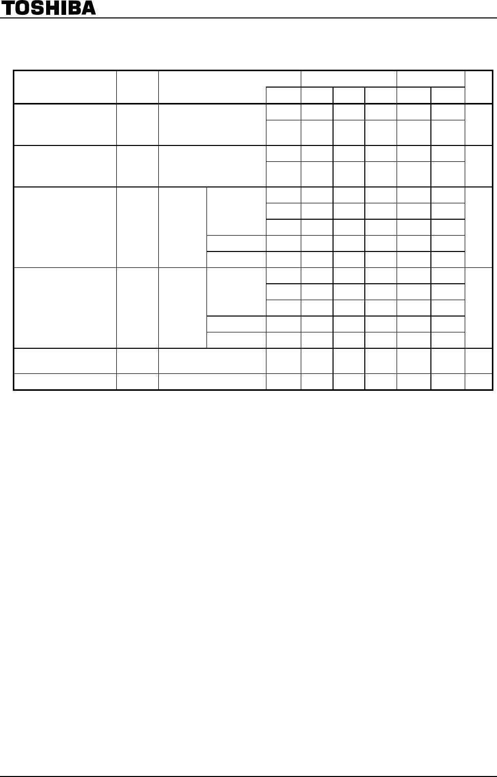
Absolute Maximum Ratings
(Ta
=
25°C)
Characteristics Symbol Rating Unit
Supply voltage V
CC
−0.5 to 7.0 V
DC input voltage V
IN
−0.5 to 7.0 V
DC output voltage V
OUT
−0.5 to V
CC
+ 0.5 V
Input diode current I
IK
−20 mA
Output diode current I
OK
±20 (Note1) mA
DC output current I
OUT
±25 mA
DC V
CC
/ground current I
CC
±50 mA
300 (SM8)
Power dissipation P
D
200 (US8)
mW
Storage temperature T
stg
−65 to 150 °C
Lead temperature (10 s) T
L
260 °C
Note: Using continuously under heavy loads (e.g. the application of high temperature/current/voltage and the
significant change in temperature, etc.) may cause this product to decrease in the reliability significantly even if
the operating conditions (i.e. operating temperature/current/voltage, etc.) are within the absolute maximum
ratings and the operating ranges.
Please design the appropriate reliability upon reviewing the Toshiba Semiconductor Reliability Handbook
(“Handling Precautions”/“Derating Concept and Methods”) and individual reliability data (i.e. reliability test report
and estimated failure rate, etc).
Note 1: V
OUT
< GND, V
OUT
> V
CC
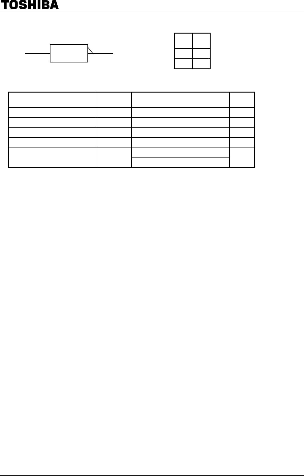
TC7WH04FU
TC7WH04FK
Weight
SSOP8-P-0.65: 0.02 g (typ.)
SSOP8-P-0.50A: 0.01 g (typ.)
SM8 US8
Product Name
H 0 4
Lot No.
W H
0 4
8 V
CC
GND 4
6 3A
5 Y2
1A 1
3Y 2
2A 3
7 1Y
(SM8)
(US8)
Pin Assignment (top view)