ZXBM1004Q16TA

1
SEMICONDUCTORS
DESCRIPTION
The ZXBM1004 is a single-phase, DC brushless motor pre-driver with PWM
variable speed control suitable for fan and blower motors. The controller is
intended for applications where the fan or blower speed is controlled by an
external PWM signal, thermistor or DC voltage.
FEATURES
Compliant with external PWM speed control
Compliant with thermistor control
Minimum speed setting
Low noise
Auto restart
Built in hall amplifier
Speed pulse (FG) and lock rotor (RD) outputs
Up to 18V input voltage (60V with external regulator)
QSOP16 package
Associated application notes:-
AN41 - Thermistor control
AN42 - External PWM control
AN43 - Interfacing to the motor windings
APPLICATIONS
Mainframe and personal computer fans and blowers
Instrumentation fans
Central heating blowers
Automotive climate control
DEVICE MARKING
ZETEX
ZXBM
1004
ZXBM1004
ISSUE 6 - MAY 2007
VARIABLE SPEED SINGLE-PHASE BLDC MOTOR CONTROLLER
DEVICE
REEL SIZE TAPE WIDTH QUANTITY PER REEL
ZXBM1004Q16TA
ZXBM1004Q16TC
7" (180mm)
13" (330mm)
12mm
12mm
500
2,500
ORDERING INFORMATION - QSOP16
Q
S
O
P
1
6
ZXBM1004
SEMICONDUCTORS
ISSUE 6 - MAY 2007
2
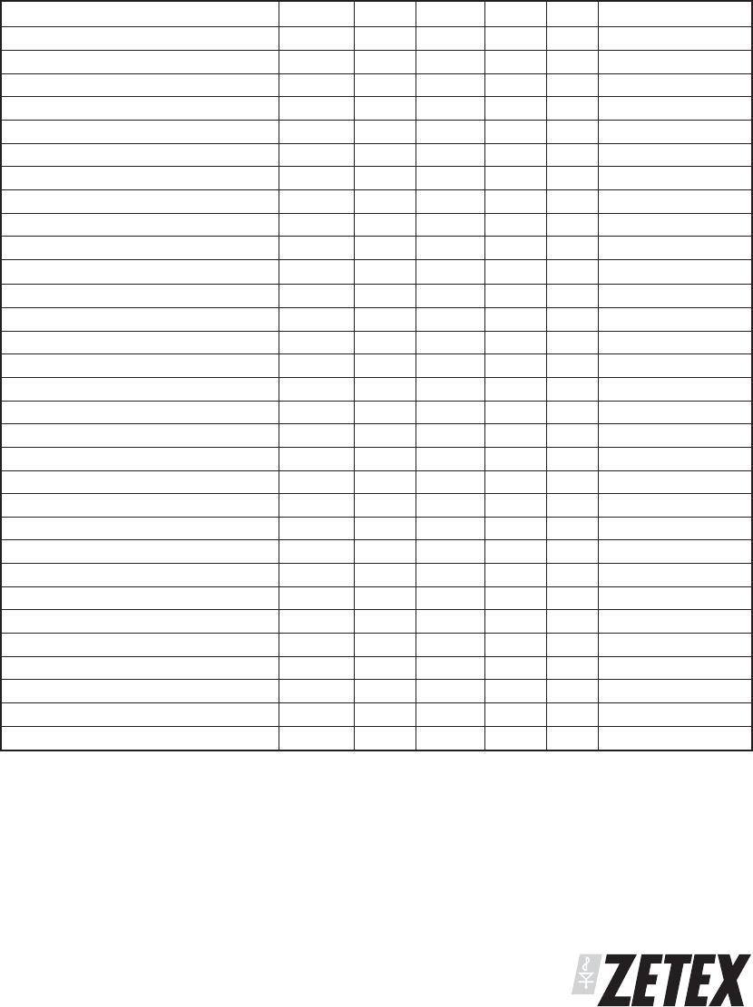
PARAMETER SYMBOL LIMITS UNIT
Supply voltage V
CCmax
-0.6 to 20 V
Input current I
CCmax
200 mA
Input voltage V
IN
max
-0.5 to V
CC
+0.5 V
Output voltage V
OUT
max
-0.5 to V
CC
+0.5 V
Power dissipation P
Dmax
500 mW
Operating temp. T
OPR
-40 to 110 C
Storage temp. T
STG
-55 to 150 C
ABSOLUTE MAXIMUM RATINGS
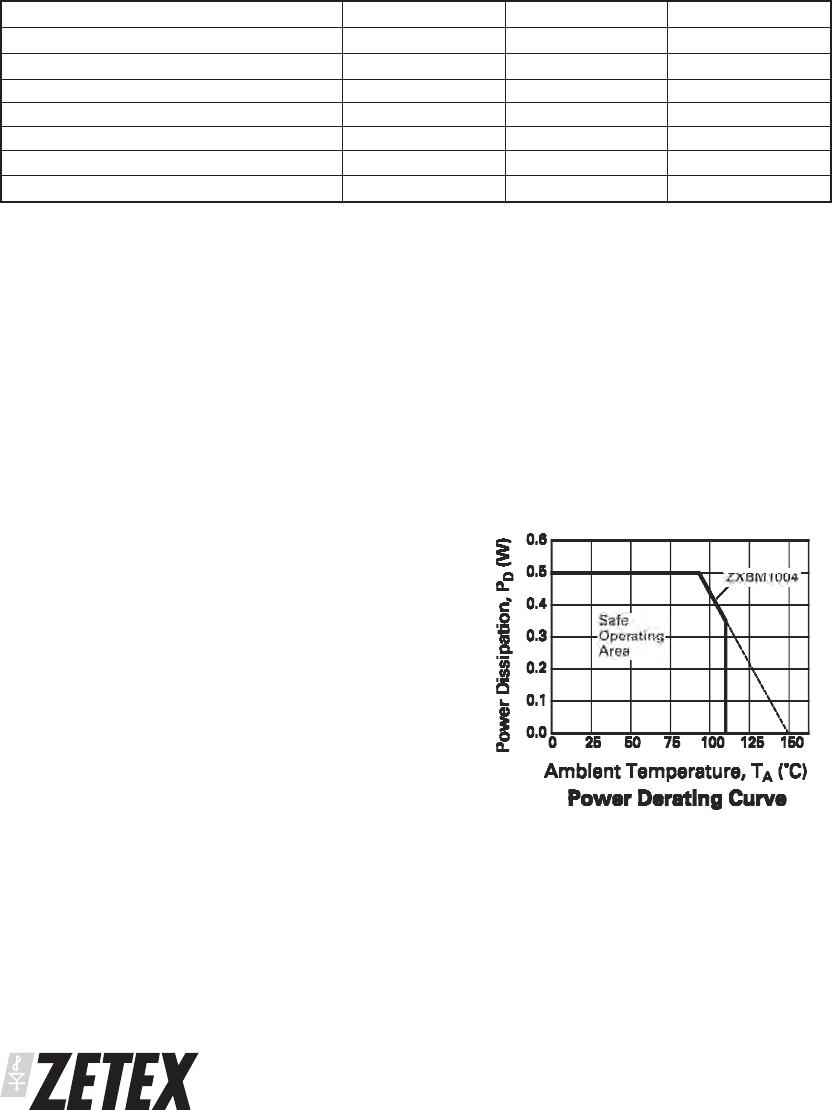
Power Dissipation
1) Maximum allowable Power Dissipation, P
D
,
is shown plotted against Ambient Temperature,
T
A
, in the accompanying Power Derating Curve,
indicating the Safe Operating Area for the device.
2) Power consumed by the device, P
T
, can be
calculated from the equation:
P
T
= P
Q
+ P
PhHi
+ P
PhLo
where P
Q
is power dissipated under quiescent
current conditions, given by:
P
Q
= Vcc x Icc
where Vcc is the application
device Supply Voltage
and Icc is the maximum Supply
Current given in the Electrical
Characteristics
and P
PhHi
is power generated due to either one of
the phase outputs Ph1Hi or Ph2Hi being
active, given by:
P
PhHi
= I
OL
x V
OL
where I
OL
is the application Ph1Hi and Ph2Hi
output currents
and V
OL
is the maximum Low Level
Output Voltage for the Ph1Hi and
Ph2Hi outputs given in the Electrical
Characteristics
and P
PhLo
is power generated due to either one of
the phase outputs Ph1Lo or Ph2Lo being
active, given by:
P
PhLo
= I
OH
x (V
CC
- V
OH
)
where I
OH
is the application Ph1Lo and Ph2Lo
output currents
and Vcc is the application device Supply
Voltage
and V
OH
is the minimum High Level
Output Voltage for the Ph1Lo and
Ph2Lo outputs given in the Electrical
Characteristics
ZXBM1004
SEMICONDUCTORS
ISSUE 6 - MAY 2007
3
PARAMETER SYMBOL
MIN. TYP. MAX. UNIT
CONDITIONS
Supply voltage V
CC
4.7 18 V
Supply current I
CC
6 8.5 mA No load
(1)
Hall amp input voltage V
IN
40 mV diff p-p
Hall amp common mode voltage V
CM
0.5 V
CC
-1.5 V
Hall amp input offset V
OFS
7mV
Hall amp bias current I
BS
400 650 nA
Ph1Lo, Ph2Lo output high voltage
V
OH
V
CC
-2.2 V
CC
-1.8 V I
OH
=80mA
Ph1Lo, Ph2Lo output low voltage
V
OLA
0.4 0.6 V I
OL
=16mA
(2)
Ph1Lo, Ph2Lo output low voltage
V
OLB
0.4 0.6 V I
OL
=50A
(3)
Ph1Lo, Ph2Lo output source current
I
OH
-80 mA
Ph1Lo, Ph2Lo output sink current
I
OL
16 mA
Ph1Hi, Ph2Hi output low voltage
V
OL
0.5 0.7 V
I
OL
=100mA
Ph1Hi, Ph2Hi output sink current
I
OL
100 mA
C
PWM
charge current
I
PWMC
-6.2 -7.6 -9 A
C
PWM
discharge current I
PWMD
65 80 95 A
C
PWM
high threshold voltage V
THH
2.9533.15V
C
PWM
low threshold voltage V
THL
0.9411.11V
PWM frequency F
PWM
24 kHz
C
PWM
=0.1nF
ThRef voltage V
ThRef
2.925 3.0 3.14 V
I
OThRef
=-100A
ThRef output current I
OThRef
-0.2 -1 mA
S
MIN
input current I
ISMIN
-0.25 -0.5 A
Vin = 2V
SPD voltage minimum V
SPDL
1V
100% PWM drive
SPD voltage maximum V
SPDH
3V
0% PWM drive
SPD input current I
ISPD
-0.8 -2 A
Vin = 2V
C
LCK
charge current I
LCKC
-2 -3 A
C
LCK
discharge current I
LCKD
0.2 0.35 A
C
LCK
high threshold voltage V
THH
3V
C
LCK
low threshold voltage V
THL
1V
Lock condition On:Off ratio
1:12
FG & RD output current I
OL
5mA
FG & RD low level output voltage V
OL
0.5 V
I
OI
=5mA
ELECTRICAL CHARACTERISTICS (at T
amb
= 25°C & V
CC
= 12V)
Notes:
(1) Measured with pins H+, H-, C
LCK
and C
PWM
= 0V and all other signal pins open circuit.
(2) Measured when opposing phase output is low.
(3) Measured when opposing phase output is high.

ZXBM1004Q16TA

Mfr. #:
Manufacturer:
Diodes Incorporated
Description:
Motor / Motion / Ignition Controllers & Drivers Var Spd Sngl-p BLDC Mtr PreDrvr w/ Min
Lifecycle:
New from this manufacturer.
Delivery:
DHL FedEx Ups TNT EMS
Payment:
T/T Paypal Visa MoneyGram Western Union

Products related to this Datasheet