ZXBM1004Q16TA

ZXBM1004
SEMICONDUCTORS
ISSUE 6 - MAY 2007
4
Block diagram
Vcc
SPD
H+
H-
Gnd
Ph1Lo
Ph2Lo
C
PWM
CLCK
FG
ZXBM1004
QSOP16
RD
V+OP
ThRef
S
MIN
1
Ph1Hi
Ph2Hi
Pin assignments
PIN FUNCTIONAL DESCRIPTION
H+ - Hall input
H- - Hall input
The rotor position is detected by a Hall sensor, with the
output applied to the H+ and H- pins. This sensor can be
either a 4 pin 'naked' Hall device or of the 3 pin buffered
switching type. For a 4 pin device the differential Hall
output signal is connected to the H+ and H- pins. For a
buffered Hall sensor the Hall device output is attached
to the H+ pin, with a pull-up attached if needed, whilst
the H- pin has an external potential divider attached to
hold the pin at half V
cc
. When H+ is high in relation to H-,
Ph2 is the active drive.
ThRef - Network Reference
This is a reference voltage of nominal 3V. It is designed
for the ability to 'source' and therefore it will not 'sink'
any current from a higher voltage.
The total current drawn from the pin by the minimum
speed potential divider to pin S
MIN
and any voltage
setting network should not exceed 1mA at maximum
temperature.
SPD - Speed Control Input
The voltage applied to the SPD pin provides control
over the Fan Motor speed by varying the Pulse Width
Modulated (PWM) drive ratio at the Ph1Lo and Ph2Lo
outputs. The control signal takes the form of a voltage
input of range 3V to 1V, representing 0% to 100% drive
respectively.
If variable speed control is not required this pin can be
left with an external potential divider to set a fixed
speed or tied to ground to provide full speed i.e. 100%
PWM drive.
If required this pin can also be used as an enable pin.
The application of a voltage >3.0V will force the PWM
drive fully off, in effect disabling the drive.
S
MIN
- Sets Minimum Speed
A voltage can be set on this pin via a potential divider
between the ThRef and Gnd. This voltage is monitored
by the SPD pin such that it cannot rise above it. As a
higher voltage on the SPD pin represents a lower speed
it therefore restricts the lower speed range of the fan. If
this feature is not required the pin is left tied to ThRef so
no minimum speed will be set.
If the fan is being controlled from an external voltage
source onto the SPD pin then either this feature should
not be used or if it is required then a >1k resistor
should be placed in series with the SPD pin.
C
PWM
- Sets PWM Frequency
This pin has an external capacitor attached to set the
PWM frequency for the Phase drive outputs. A
capacitor value of 0.1nF will provide a PWM frequency
of typically 24kHz.
The C
PWM
timing period (T
PWM
) is determined by the
following equation:
T
VVxC
I
VVxC
I
PWM
THH THL
PWMC
THH THL
PWMD
=
+
()()
Where: C = C
PWM
+15, in pF
V
THH
and V
THL
are the C
PWM
pin
threshold voltages
I
PWMC
and I
PWMD
are the charge and
discharge currents in A.
T
PWM
is in ms
ZXBM1004
SEMICONDUCTORS
ISSUE 6 - MAY 2007
5
As these threshold voltages are nominally set to V
THH
=
3V and V
THL
= 1V the equations can be simplified as
follows:
T
C
I
C
I
PWM
PWMC PWMD
=+
22
C
LCK
- Locked rotor timing capacitor
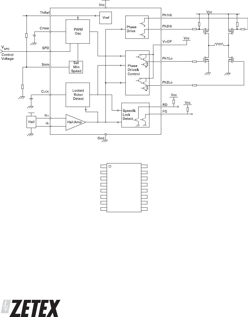
Should the fan stop rotating for any reason, i.e. an
obstruction in the fan blade or a seized bearing, then
the device will enter a Rotor Locked condition. In this
condition after a predetermined time (T
LOCK
) the RD pin
will go high and the Phase outputs will be disabled.
After a further delay (T
OFF
) the controller will re-enable
the Phase drive for a defined period (T
ON
) in an attempt
to re-start the fan. This cycle of (T
OFF
) and (T
ON
) will be
repeated indefinitely or until the fan re-starts.
GND - Ground
This is the device supply ground return pin and will
generally be the most negative supply pin to the fan.
RD - Locked Rotor error output
This pin is the Locked Rotor output as referred to in the
C
LCK
timing section above. It is high when the rotor is
stopped and low when it is running.
This is an open collector drive giving an active pull
down with the high level being provided by an external
pull up resistor.
FG - Frequency Generator (speed) output
This is the Frequency Generator output and is a
buffered signal from the Hall sensor.
This is an open collector drive giving an active pull
down with the high level being provided by an external
pull up resistor.
Ph1Lo & Ph2Lo - Low-side External
H-bridge Driver
This pair of outputs drive the Low side of the external
high power H-bridge devices which in turn drives the
single phase winding. These outputs provide both the
commutation and PWM waveforms. The outputs are of
the Darlington emitter follower type with an active
pull-down to help faster switch off when using bipolar
devices. When in the high state the outputs will provide
up to 80mA of drive into the base or gates of external
transistors as shown in the Typical Application circuit
following.
When in the low state the active Phase drive is capable
of sinking up to 16mA when driving low to aid turn off
times during PWM operation. When the Phase is
inactive the output is held low by an internal pull-down
resistor.
Ph1Hi & Ph2Hi - High-side External H-bridge
Driver
These are the High side outputs to the external
H-bridge and are open collector outputs capable of
sinking 100mA. This signal provides commutation only
to the H-bridge.
V+OP - Phase Outputs Supply Voltage
This pin is the supply to the Phase outputs and will be
connected differently dependant upon external
transistor type.
For bipolar devices this pin will be connected by a
resistor to the V
CC
pin. The resistor is used to control
the current into the transistor base so its value is
chosen accordingly.
For MOSFET devices the pin will connect directly to the
V
CC
pin.
ZXBM1004
SEMICONDUCTORS
ISSUE 6 - MAY 2007
6

ZXBM1004Q16TA

Mfr. #:
Manufacturer:
Diodes Incorporated
Description:
Motor / Motion / Ignition Controllers & Drivers Var Spd Sngl-p BLDC Mtr PreDrvr w/ Min
Lifecycle:
New from this manufacturer.
Delivery:
DHL FedEx Ups TNT EMS
Payment:
T/T Paypal Visa MoneyGram Western Union

Products related to this Datasheet