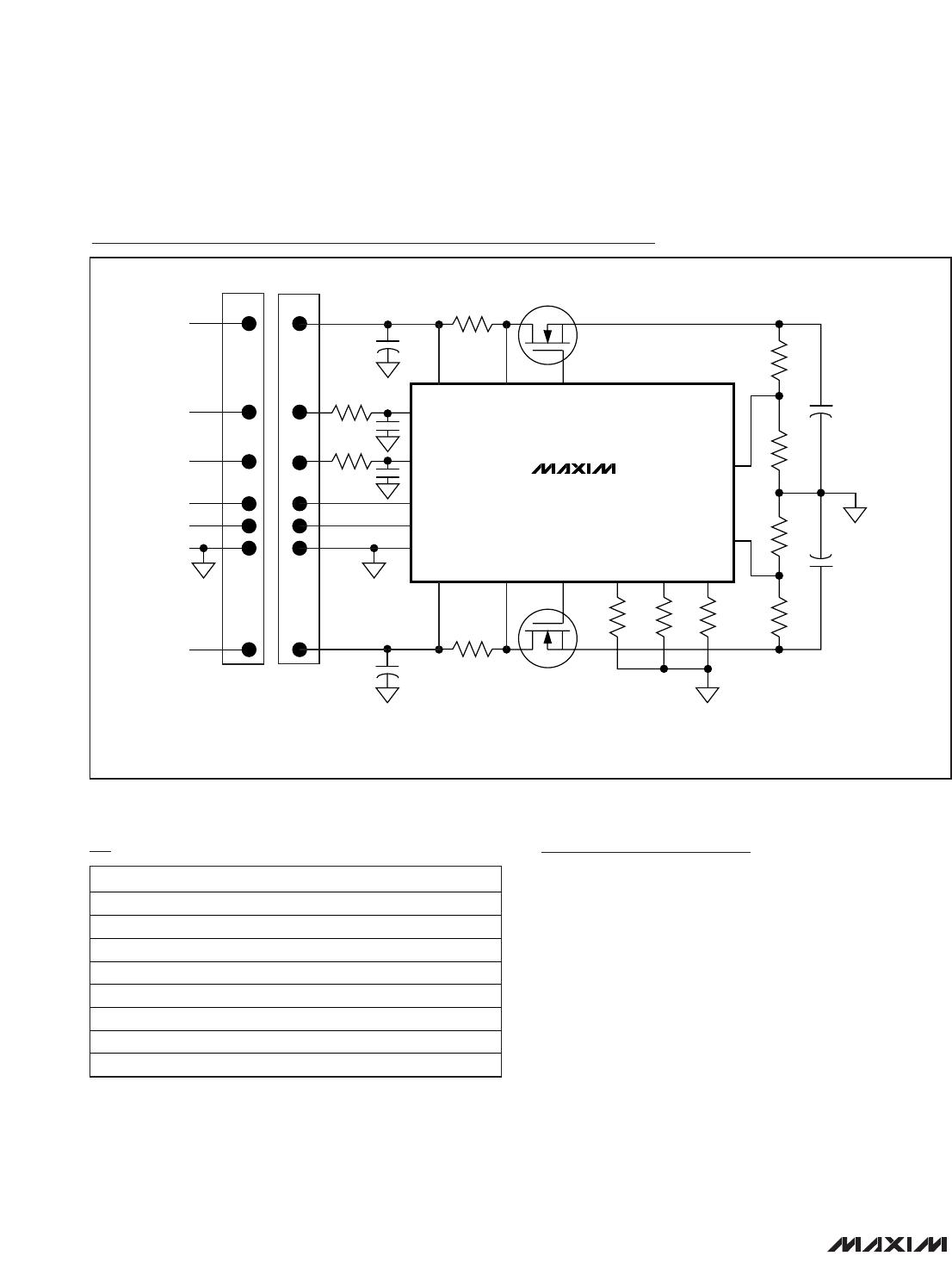
Layout Considerations
To take full advantage of the switch response time to an
output fault condition, it is important to keep all traces as
short as possible and to maximize the high-current trace
dimensions to reduce the effect of undesirable parasitic
resistance and inductance. Place the MAX5955/
MAX5956 close to the card’s connector, and a 0.01µF
capacitor to GND should be placed as close as possible
to each V
IN
pin. Use a ground plane to minimize imped-
ance and inductance. Minimize the current-sense resis-
tor trace length (< 10mm), and ensure accurate current
sensing with Kelvin connections (Figure 6).
When the output is short circuited, the voltage drop
across the external MOSFET becomes large. Hence,
the power dissipation across the switch increases, as
does the die temperature. An efficient way to achieve
good power dissipation on a surface-mount package is
to lay out two copper pads directly under the MOSFET
package on both sides of the board. Connect the two
pads to the ground plane through vias, and use
enlarged copper mounting pads on the top side of the
board (refer to the MAX5956 EV Kit data sheet).
MAX5955/MAX5956
Low-Voltage, Dual Hot-Swap Controllers with
Independent On/Off Control
______________________________________________________________________________________ 13
* REQUIRED COMPONENTS. SEE THE ON_ COMPARATORS SECTION.