MAX5955/MAX5956
Detailed Description
The MAX5955 and MAX5956 are circuit breaker ICs for
hot-swap applications where a line card is inserted into
a live backplane. The MAX5955 and MAX5956 operate
down to 1V provided one of the inputs is above 2.7V.
Normally, when a line card is plugged into a live back-
plane, the card’s discharged filter capacitors provide
low impedance that can momentarily cause the main
power supply to collapse. The MAX5955 and MAX5956
reside either on the backplane or on the removable
card to provide inrush current limiting and short-circuit
protection. This is achieved by using external n-chan-
nel MOSFETs, external current-sense resistors, and two
on-chip comparators. The startup period and current-
limit threshold of the MAX5955/MAX5956 can be
adjusted with external resistors. Figure 1 shows the
MAX5955/MAX5956 functional diagram.
The MAX5955/MAX5956 pull both PGOODs low and
both external FETs off for an overcurrent condition. The
MAX5955 also pulls both PGOODs low and both external
FETs off (protection) for an undervoltage/overvoltage
fault, whereas, the MAX5956 ONLY pulls the corre-
sponding fault channel’s PGOOD_ low (monitoring).
When the overvoltage/undervoltage fault disappears on
the MAX5956, the corresponding PGOOD_ automatically
goes high impedance.
Low-Voltage, Dual Hot-Swap Controllers with
Independent On/Off Control
6 _______________________________________________________________________________________
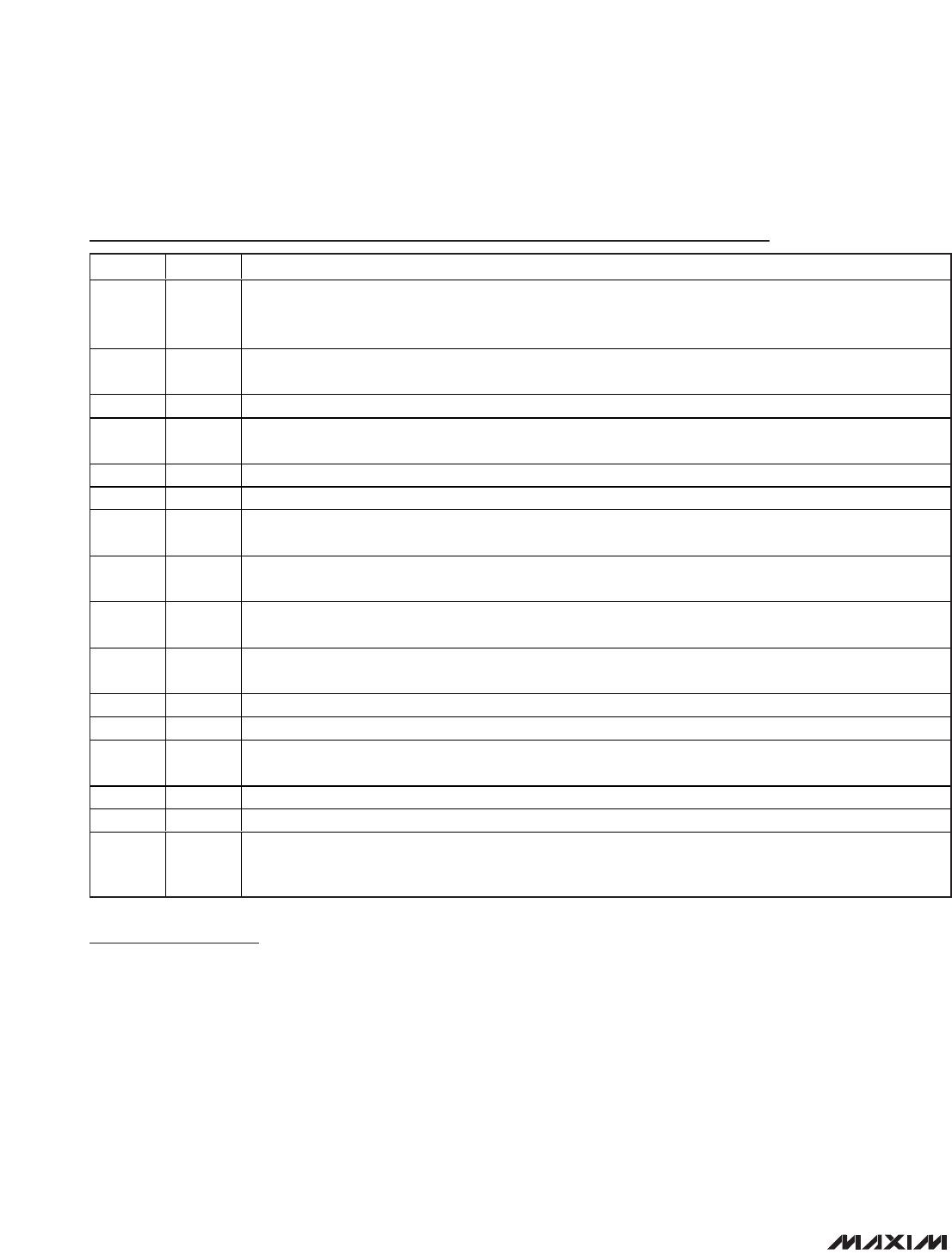
Pin Description
PIN NAME FUNCTION
1 PGOOD1
Channel 1 Status Output (Open Drain, see the Absolute Maximum Ratings). PGOOD1 asserts high when hot
swap is successful and channel 1 is within regulation. PGOOD1 asserts low during startup, when ON1 is
low, when channel 1 is off, or when channel 1 has any fault condition.
2 TIM
Startup Timer Setting. Connect a resistor from TIM to GND to set the startup period. Leave TIM unconnected
for the default startup period of 9ms.
3 IN1 Channel 1 Supply Input. Connect to a supply voltage of 1V to 13.2V.
4 SENSE1
Channel 1 Current-Sense Input. Connect R
SENSE1
from IN1 to SENSE1. Connect to IN1 to disable circuit
breaker function of channel 1.
5 GATE1 Channel 1 Gate-Drive Output. Connect to the gate of an external n-channel MOSFET.
6 GND Ground
7 LIM1
Channel 1 Current-Limit Setting. Connect a resistor from LIM1 to GND to set the current trip level. Connect to
GND for the default 25mV threshold (see the Slow-Comparator Threshold, R
LIM
section).
8 MON1
Channel 1 Output-Voltage Monitor. Window comparator input. Connect through a resistive divider from
OUT1 to GND to set the channel 1 overvoltage and undervoltage threshold. Connect to IN1 to disable.
9 MON2
Channel 2 Output-Voltage Monitor. Window comparator input. Connect through a resistive divider from
OUT2 to GND to set the channel 2 overvoltage and undervoltage threshold. Connect to IN2 to disable.
10 LIM2
Channel 2 Current-Limit Setting. Connect a resistor from LIM2 to GND to set the current trip level. Connect to
GND for the default 25mV threshold (see the Slow-Comparator Threshold, R
LIM
section).
11 ON1 Channel 1 On/Off Control Input. Channel 1 is turned on when V
ON1
> 0.875V.
12 GATE2 Channel 2 Gate-Drive Output. Connect to the gate of an external n-channel MOSFET.
13 SENSE2
Channel 2 Current-Sense Input. Connect R
SENSE2
from IN2 to SENSE2. Connect to IN2 to disable circuit-
breaker function of channel 2.
14 IN2 Channel 2 Supply Input. Connect to a supply voltage of 1V to 13.2V.
15 ON2 Channel 2 On/Off Control Input. Channel 2 is turned on when V
ON2
> 0.875V.
16 PGOOD2
Channel 2 Status Output (Open Drain, see the Absolute Maximum Ratings). PGOOD2 asserts high when hot
swap is successful and channel 2 is within regulation. PGOOD2 asserts low during startup, when V
ON2
is
low, when channel 2 is off, or when channel 2 has any fault condition.

