16
LTC1553L
Feedback Loop Compensation
The LTC1553L voltage feedback loop is compensated at
the COMP pin, attached to the output node of the internal
g
m
error amplifier. The feedback loop can generally be
compensated properly with an RC + C network from COMP
to GND as shown in Figure 8a.
Loop stability is affected by the values of the inductor,
output capacitor, output capacitor ESR, error amplifier
transconductance and error amplifier compensation net-
work. The inductor and the output capacitor create a
double pole at the frequency:
f
LC
=
1
2π√(L
O
)(C
OUT
)
The ESR of the output capacitor forms a zero at the
frequency:
f
ESR
=
1
2π(ESR)(C
OUT
)
The compensation network at the error amplifier output is
to provide enough phase margin at the 0dB crossover
frequency for the overall closed-loop transfer function.
The zero and pole from the compensation network are:
f
Z
=
1
2π(R
C
)(C
C
)
and
f
P
=
1
2π(R
C
)(C1)
respectively.
Figure 8b shows the Bode plot of the overall transfer
function.
The compensation value used in this design is based on
the following criteria: f
SW
= 12f
CO
, f
Z
= f
LC
and f
P
= 5f
CO
. At
the closed-loop frequency f
CO
, the attenuation due the LC
filter and the input resistor divider is compensated by the
gain of the PWM modulator and the gain of the error
amplifier (g
mERR
)(R
C
). Although a mathematical approach
to frequency compensation can be used, the added
complication of input and/or output filters, unknown ca-
pacitor ESR, and gross operating point changes with input
voltage, load current variations, all suggest a more prac-
tical empirical method. This can be done by injecting a
transient current at the load and using an RC network box
to iterate toward the final compensation values, or by
obtaining the optimum loop response using a network
analyzer to find the actual loop poles and zeros.
APPLICATIONS INFORMATION
WUU
U
Figure 8a. Compensation Pin Hook-Up
1553L F08a
DAC
LTC1553L
SENSE
COMP
R
C
C
C
C1
+
ERR
6
10
Figure 8b. Bode Plot of the LTC1553L Overall Transfer Function
20dB/DECADE
LOOP GAIN
f
P
f
Z
f
CO
f
ESR
FREQUENCY
1553L F08b
f
SW
= LTC1553L SWITCHING 
FREQUENCY
f
CO
= CLOSED-LOOP CROSSOVER 
FREQUENCY
f
LC
Table 6. Suggested Compensation Network for 5V Input
Application Using Multiple Paralleled 330µF AVX TPS Output
Capacitors
L
O
(
µ
H) C
O
(
µ
F) R
C
(k
)C
C
(
µ
F) C1 (pF)
1 990 1.8 0.022 680
1 1980 3.6 0.01 330
1 4950 9.1 0.01 120
2.7 990 5.1 0.01 220
2.7 1980 10 0.01 120
2.7 4950 24 0.0047 47
5.6 990 10 0.01 120
5.6 1980 20 0.0047 56
5.6 4950 51 0.0036 22
17
LTC1553L
APPLICATIONS INFORMATION
WUU
U
this happens, FAULT will be triggered. Once FAULT is
triggered, G1 and G2 will be forced low immediately and
the LTC1553L will remain in this state until V
CC
power
supply is recycled or OUTEN is toggled.
Table 6 shows the suggested compensation components
for 5V input applications based on the inductor and output
capacitor values. The values were calculated using mul-
tiple paralleled 330µF AVX TPS series surface mount
tantalum capacitors as the output capacitor. The optimum
component values might deviate from the suggested
values slightly because of board layout and operating
condition differences.
An alternate output capacitor is the Sanyo MV-GX series.
Using multiple parallel 1500µF Sanyo MV-GX capacitors
for the output capacitor, Table 7 shows the suggested
compensation component value for a 5V input application
based on the inductor and output capacitor values.
Table 7. Suggested Compensation Network for 5V Input
Application Using Multiple Paralleled 1500µF SANYO MV-GX
Output Capacitors
L
O
(
µ
H) C
O
(
µ
F) R
C
(k
)C
C
(
µ
F) C1 (pF)
1 4500 4.3 0.022 270
1 6000 5.6 0.0047 220
1 9000 8.2 0.01 150
2.7 4500 11 0.01 100
2.7 6000 15 0.01 82
2.7 9000 22 0.01 56
5.6 4500 24 0.01 56
5.6 6000 30 0.0047 39
5.6 9000 47 0.0047 27
VID0 to VID4, PWRGD and FAULT
The digital inputs (VID0 to VID4) program the internal DAC
which in turn controls the output voltage. These digital
input controls are intended to be static and are not
designed for high speed switching. Forcing V
OUT
to step
from a high to a low voltage by changing the VID
n
pins
quickly can cause FAULT to trip.
Figure 9 shows the relationship between the V
OUT
voltage,
PWRGD and FAULT. To prevent PWRGD from interrupting
the CPU unnecessarily, the LTC1553L has a built-in t
PWRBAD
delay to prevent noise at the SENSE pin from toggling
PWRGD. The internal time delay is designed to take about
500µs for PWRGD to go low and 1ms for it to recover.
Once PWRGD goes low, the internal circuitry watches for
the output voltage to exceed 115% of the rated voltage. If
RATED V
OUT
V
OUT
15%
5%
–5%
t
PWRBAD
t
PWRGD
t
FAULT
FAULT
PWRGD
1553L F09
Figure 9. PWRGD and FAULT
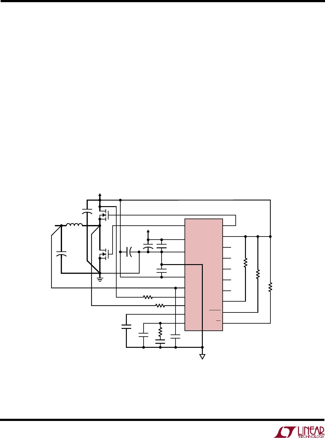
LAYOUT CONSIDERATIONS
When laying out the printed circuit board, the following
checklist should be used to ensure proper operation of the
LTC1553L. These items are also illustrated graphically in
the layout diagram of Figure 10. The thicker lines show the
high current paths. Note that at 10A current levels or
above, current density in the PC board itself is a serious
concern. Traces carrying high current should be as wide
as possible. For example, a PCB fabricated with 2oz
copper requires a minimum trace width of 0.15" to
carry 10A.
1. In general, layout should begin with the location of the
power devices. Be sure to orient the power circuitry so
that a clean power flow path is achieved. Conductor
widths should be maximized and lengths minimized.
After you are satisfied with the power path, the control
circuitry should be laid out. It is much easier to find
routes for the relatively small traces in the control
circuits than it is to find circuitous routes for high
current paths.
2. The GND and SGND pins should be shorted right at the
LTC1553L. This helps to minimize internal ground
disturbances in the LTC1553L and prevents differences
in ground potential from disrupting internal circuit
operation. This connection should then tie into the
18
LTC1553L
APPLICATIONS INFORMATION
WUU
U
capacitors shown at V
CC
and PV
CC
will help provide
optimum regulation performance.
5. The (+) plate of C
IN
should be connected as close as
possible to the drain of the upper MOSFET. An addi-
tional 1µF ceramic capacitor between V
IN
and power
ground is recommended.
6. The SENSE pin is very sensitive to pickup from the
switching node. Care should be taken to isolate SENSE
from possible capacitive coupling to the inductor switch-
ing signal. A 0.1µF is required between the SENSE pin
and the SGND pin next to the LTC1553L.
7. OUTEN is a high impedance input and should be
externally pulled up to a logic HIGH for normal
operation.
8. Kelvin sense I
MAX
and I
FB
at Q1 drain and source pins.
ground plane at a single point, preferably at a fairly quiet
point in the circuit such as close to the output capaci-
tors. This is not always practical, however, due to
physical constraints. Another reasonably good point to
make this connection is between the output capacitors
and the source connection of the low side FET Q2. Do
not tie this single point ground in the trace run between
the low side FET source and the input capacitor ground,
as this area of the ground plane will be very noisy.
3. The small signal resistors and capacitors for frequency
compensation and soft start should be located very
close to their respective pins and the ground ends
connected to the signal ground pin through a separate
trace. Do not connect these parts to the ground plane!
4. The V
CC
and PV
CC
decoupling capacitors should be as
close to the LTC1553L as possible. The 10µF bypass
Figure 10. LTC1553L Layout Diagram
10µF
10µF
5.6k
1153L F10
0.1µF
SGND
G1
OUTEN
VID0
VID1
VID2
VID3
VID4
20
19
18
17
16
15
14
13
12
11
G2
PV
CC
V
CC
SENSE
0.1µF
+
+
V
OUT
L
O
PV
CC
R
C
R
IMAX
BOLD LINES INDICATE
HIGH CURRENT PATHS
C
C
C1
C
SS
C
OUT
Q1
Q2
+
C
IN
V
IN
5.6k
5.6k
LTC1553L
R
IFB
+
3
1
2
4
5
6
7
8
9
10
GND
I
MAX
I
FB
SS
COMP
VID0
VID1
VID2
VID3
VID4
PWRGD
FAULT
OT
0.1µF

LTC1553LCSW#TRPBF

Mfr. #:
Manufacturer:
Analog Devices / Linear Technology
Description:
Switching Voltage Regulators 5-B Progmable Sync Sw Reg Cntr for Penti
Lifecycle:
New from this manufacturer.
Delivery:
DHL FedEx Ups TNT EMS
Payment:
T/T Paypal Visa MoneyGram Western Union