7
LTC1553L
PIN FUNCTIONS
UUU
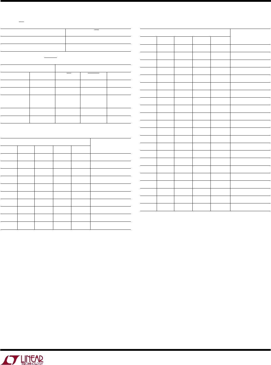
VID0, VID1, VID2, VID3, VID4 (Pins 18, 17, 16, 15, 14):
Digital Voltage Select. TTL inputs used to set the regulated
output voltage required by the processor (Table 3). There
is an internal 20kΩ pull-up at each pin. When all five VID
n
pins are high or floating, the chip will shut down.
OUTEN (Pin 19): Output Enable. TTL input which enables
the output voltage. The external MOSFET temperature can
be monitored with an external thermistor as shown in
Figure 11. When the OUTEN input voltage drops below 2V,
OT trips. As OUTEN drops below 1.7V, the drivers are
internally disabled to prevent the MOSFETs from heating
further. If OUTEN is less than 1.2V for longer than 30µs,
the LTC1553L will enter shutdown mode. The internal
oscillator can be synchronized to a faster external clock by
applying the external clocking signal to the OUTEN pin.
G1 (Pin 20): Gate Drive for the Upper N-Channel MOSFET,
Q1. This output will swing from PV
CC
to GND. It will always
be low when G2 is high or the output is disabled.
BLOCK DIAGRAM
W
VID0
VID1
VID2
VID3
VID4
18
17
16
15
14
OUTEN
19
COMP
SS
PV
CC
G1
G2
1553 BD
SENSE
–
+
FC
–
+
–+
PWM
SYSTEM
POWER
DOWN
R
S
DISDR
V
REF
I
SS
Q
SS
115% V
REF
V
REF
0.5V
REF
/
0.7V
REF
HCL MONOMHCL
V
REF
– 5% V
REF
+ 5%
DELAY
DAC
FB
LOGIC
MAX
–
+
MIN
–
+
ERR
–
+
I
MAX
I
MAX
I
FB
PWRGD
CC
–
+
LVC
FAULT
OT
BG
10
9
12
11
13
2
20
1
6
8
7