IDT 89HPES16NT16G2 Datasheet
16 of 33 December 17, 2013
T
TX-RISE
, T
TX-FALL
TX Rise/Fall Time: 20% - 80% 0.125 0.15 UI
T
TX- IDLE-MIN
Minimum time in idle 20 20 UI
T
TX-IDLE-SET-TO-
IDLE
Maximum time to transition to a valid Idle after sending
an Idle ordered set
88 ns
T
TX-IDLE-TO-DIFF-
DATA
Maximum time to transition from valid idle to diff data 8 8 ns
T
TX-SKEW
Transmitter data skew between any 2 lanes 1.3 1.3 ns
T
MIN-PULSED
Minimum Instantaneous Lone Pulse Width NA 0.9 UI
T
TX-HF-DJ-DD
Transmitter Deterministic Jitter > 1.5MHz Bandwidth NA 0.15 UI
T
RF-MISMATCH
Rise/Fall Time Differential Mismatch NA 0.1 UI
PCIe Receive
UI Unit Interval 399.88 400 400.12 199.94 200.06 ps
T
RX-EYE (with jitter)
Minimum Receiver Eye Width (jitter tolerance) 0.4 0.4 UI
T
RX-EYE-MEDIUM TO
MAX JITTER
Max time between jitter median & max deviation 0.3 UI
T
RX-SKEW
Lane to lane input skew 20 8 ns
T
RX-HF-RMS
1.5 — 100 MHz RMS jitter (common clock) NA 3.4 ps
T
RX-HF-DJ-DD
Maximum tolerable DJ by the receiver (common clock) NA 88 ps
T
RX-LF-RMS
10 KHz to 1.5 MHz RMS jitter (common clock) NA 4.2 ps
T
RX-MIN-PULSE
Minimum receiver instantaneous eye width NA 0.6 UI
1.
Minimum, Typical, and Maximum values meet the requirements under PCI Express Base Specification 2.1.
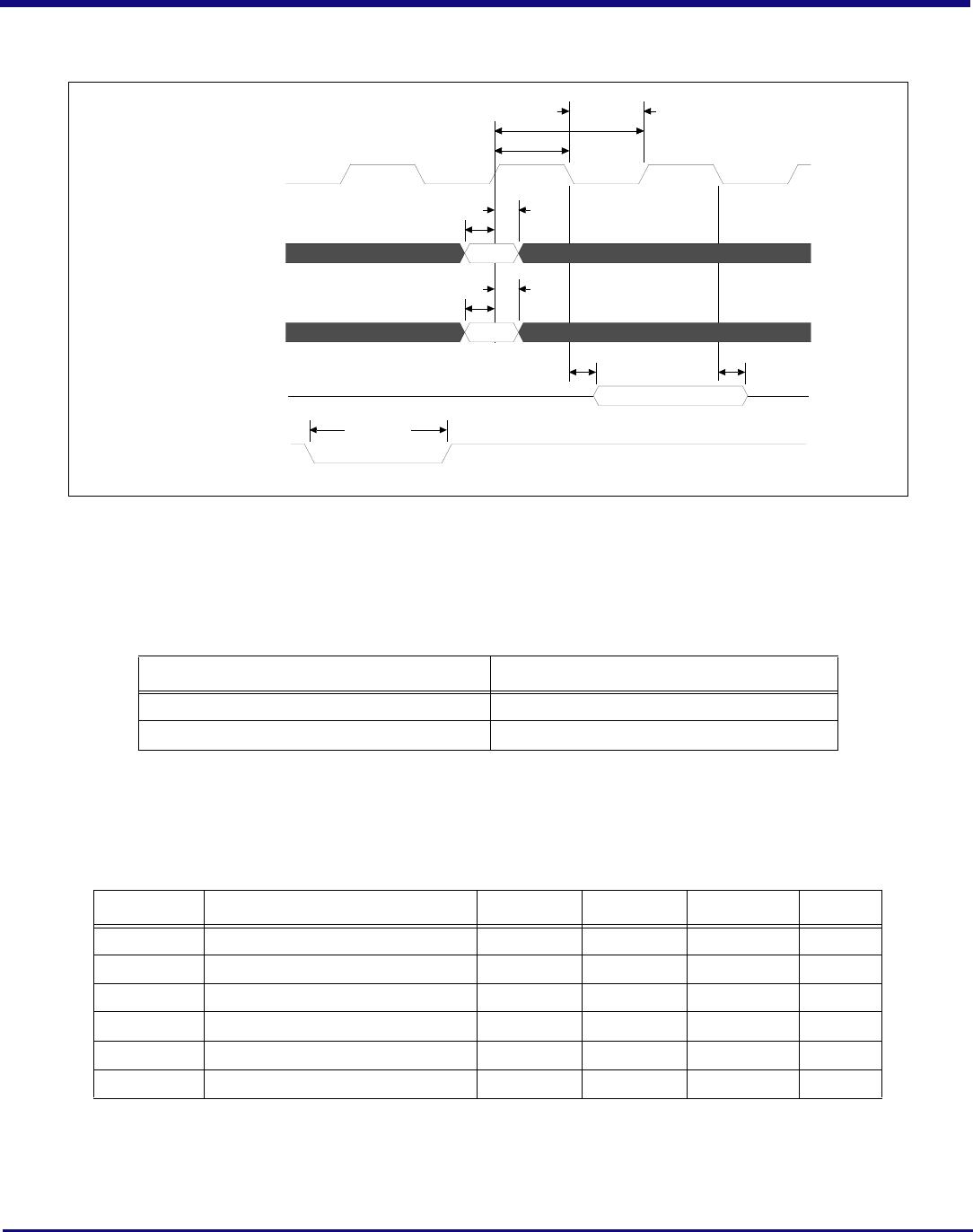
Signal Symbol
Reference
Edge
Min Max Unit
Timing
Diagram
Reference
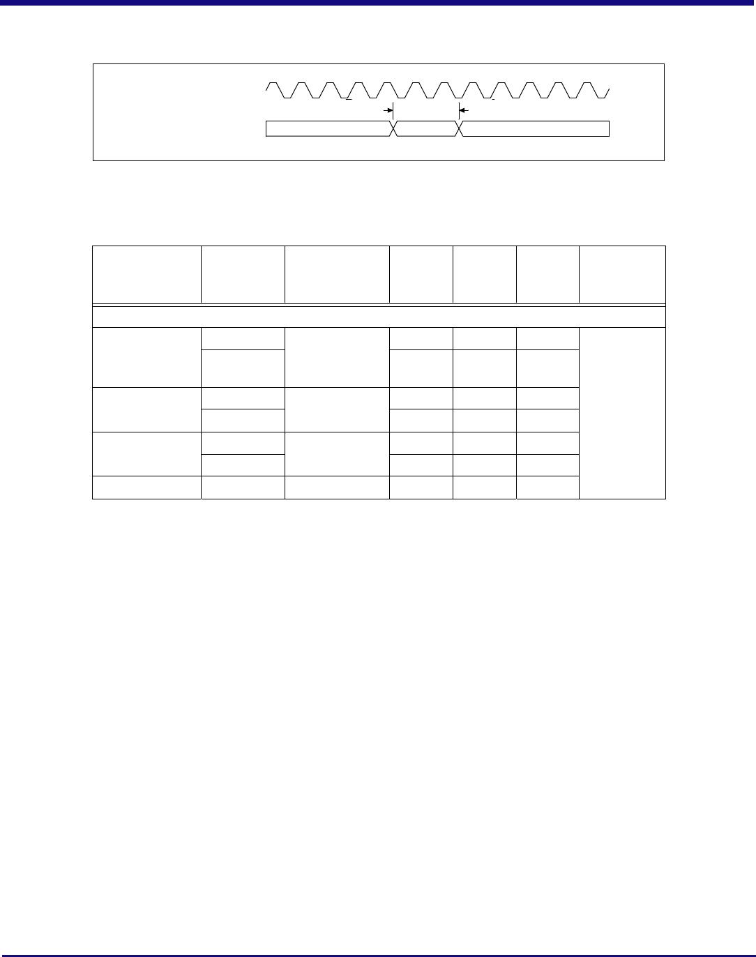
GPIO
GPIO[8:0]
1
1.
GPIO signals must meet the setup and hold times if they are synchronous or the minimum pulse width if they
are asynchronous.
Tpw_13b
2
2.
The values for this symbol were determined by calculation, not by testing.
None 50 — ns See Figure 4.
Table 13 GPIO AC Timing Characteristics
Parameter Description
Gen 1 Gen 2
Units
Min
1
Typ
1
Max
1
Min
1
Typ
1
Max
1
Table 12 PCIe AC Timing Characteristics (Part 2 of 2)