IDT 89HPES16NT16G2 Datasheet
22 of 33 December 17, 2013
Serial Link
(cont.)
PCIe Receive
V
RX-DIFFp-p
Differential input voltage (peak-
to-peak)
175 1200 120 1200 mV
RL
RX-DIFF
Receiver Differential Return
Loss
10 10 dB 0.05 - 1.25GHz
8 1.25 - 2.5GHz
RL
RX-CM
Receiver Common Mode Return
Loss
66dB
Z
RX-DIFF-DC
Differential input impedance
(DC)
80 100 120 Refer to return loss spec
Z
RX--DC
DC common mode impedance 40 50 60 40 60
Z
RX-COMM-DC
Powered down input common
mode impedance (DC)
200k 350k 50k
Z
RX-HIGH-IMP-
DC-POS
DC input CM input impedance
for V>0 during reset or power
down
50k 50k
Z
RX-HIGH-IMP-
DC-NEG
DC input CM input impedance
for V<0 during reset or power
down
1.0k 1.0k
V
RX-IDLE-DET-
DIFFp-p
Electrical idle detect threshold 65 175 65 175 mV
V
RX-CM-ACp
Receiver AC common-mode
peak voltage
150 150 mV V
RX-CM-ACp
PCIe REFCLK
C
IN
Input Capacitance 1.5 1.5 pF
Other I/Os
LOW Drive
Output
I
OL
—2.5——2.5mAV
OL
= 0.4v
I
OH
—-5.5— —-5.5 mAV
OH
= 1.5V
High Drive
Output
I
OL
—12.0— —12.0 mAV
OL
= 0.4v
I
OH
-20.0 -20.0 mA V
OH
= 1.5V
Schmitt
Trigger
Input (STI)
V
IL
-0.3 0.8 -0.3 0.8 V
V
IH
2.0 V
DD
I/O
+ 0.5
2.0 V
DD
I/O +
0.5
V—
Input V
IL
-0.3 0.8 -0.3 0.8 V
V
IH
2.0 V
DD
I/O
+ 0.5
2.0 V
DD
I/O +
0.5
V—
3.3V Output
Low Voltage
V
OL
——0.4 0.4VI
OL
= 8mA for
JTAG_TDO
and GPIO pins
3.3V Output
High Volt-
age
V
OH
2.4 2.4 V I
OH
= 8mA for
JTAG_TDO
and GPIO pins
I/O Type Parameter Description
Gen1 Gen2 Unit
Condi-
tions
Min
1
Typ
1
Max
1
Min
1
Typ
1
Max
1
Table 20 DC Electrical Characteristics (Part 2 of 3)
IDT 89HPES16NT16G2 Datasheet
23 of 33 December 17, 2013
Absolute Maximum Voltage Rating
Warning: For proper and reliable operation in adherence with this data sheet, the device should not exceed the recommended operating voltages
in Table 16. The absolute maximum operating voltages in Table 21 are offered to provide guidelines for voltage excursions outside the recommended
voltage ranges. Device functionality is not guaranteed at these conditions and sustained operation at these values or any exposure to voltages outside
the maximum range may adversely affect device functionality and reliability.
SMBus Characterization
Capacitance C
IN
8.5 8.5 pF
Leakage Inputs + 10 + 10 AV
DD
I/O (max)
I/O
LEAK W/O
Pull-ups/downs
——+ 10 + 10 AV
DD
I/O (max)
I/O
LEAK WITH
Pull-ups/downs
——+ 80 + 80 AV
DD
I/O (max)
1.
Minimum, Typical, and Maximum values meet the requirements under PCI Express Base Specification 2.1.
Core Supply
PCIe Analog
Supply
PCIe Analog
High Supply
PCIe
Transmitter
Supply
I/O Supply
1.5V 1.5V 4.6V 1.5V 4.6V
Table 21 PES16NT16G2 Absolute Maximum Voltage Rating
Symbol Parameter
SMBus 2.0 Char. Data
1
Unit
3V 3.3V 3.6V
DC Parameter for SDA Pin
V
IL
Input Low 1.16 1.26 1.35 V
V
IH
Input High 1.56 1.67 1.78 V
V
OL@350uA
Output Low 15 15 15 mV
I
OL@0.4V
23 24 25 mA
I
Pullup
Current Source A
I
IL_Leak
Input Low Leakage 0 0 0 A
I
IH_Leak
Input High Leakage 0 0 0 A
Table 22 SMBus DC Characterization Data (Part 1 of 2)
I/O Type Parameter Description
Gen1 Gen2 Unit
Condi-
tions
Min
1
Typ
1
Max
1
Min
1
Typ
1
Max
1
Table 20 DC Electrical Characteristics (Part 3 of 3)
IDT 89HPES16NT16G2 Datasheet
24 of 33 December 17, 2013
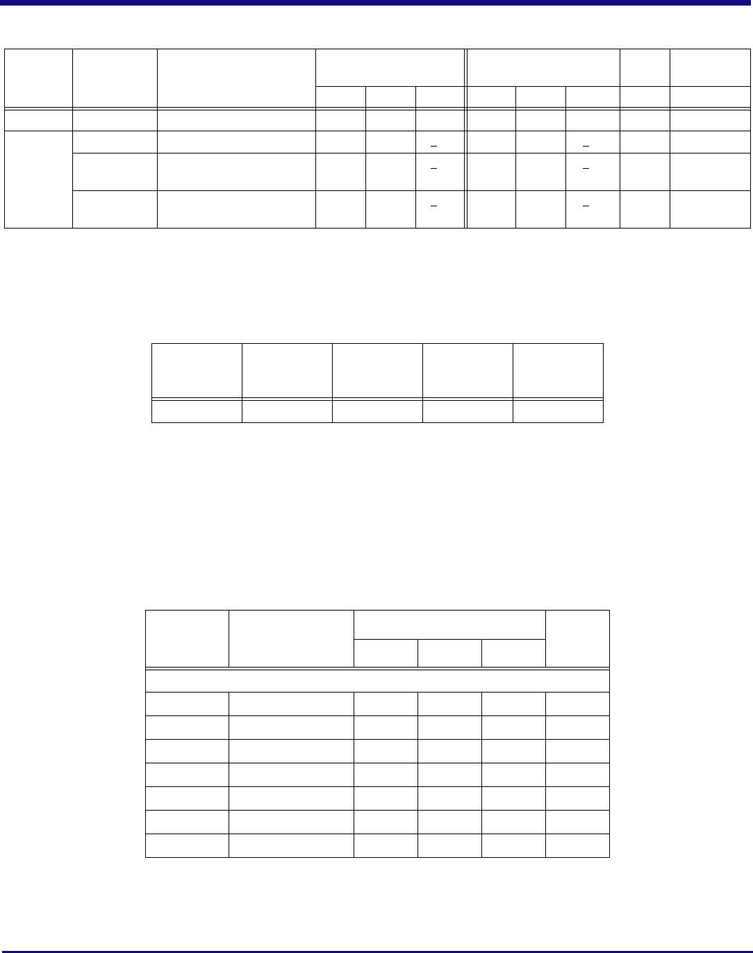
DC Parameter for SCL Pin
V
IL (V)
Input Low 1.11 1.2 1.31 V
V
IH (V)
Input High 1.54 1.65 1.76 V
I
IL_Leak
Input Low Leakage 0 0 0 A
I
IH_Leak
Input High Leakage 0 0 0 A
1.
Data at room and hot temperature.
Symbol Parameter
SMBus @3.3V ±10%
1
1.
Data at room and hot temperature.
Unit
Min Max
F
SCL
Clock frequency 5 600 KHz
T
BUF
Bus free time between Stop and
Start
3.5 s
T
HD:STA
Start condition hold time 1 s
T
SU:STA
Start condition setup time 1 s
T
SU:STO
Stop condition setup time 1 s
T
HD:DAT
Data hold time 1 ns
T
SU:DAT
Data setup time 1 ns
T
TIMEOUT
Detect clock low time out 74.7 ms
T
LOW
2
2.
T
LOW
and
T
HIGH
are measured at F
SCL
= 135 kHz.
Clock low period 3.7 s
T
HIGH
2
Clock high period 3.7 s
T
F
Clock/Data fall time 72.2 ns
T
R
Clock/Data rise time 68.3 ns
T
POR@10kHz
Time which a device must be
operational after power-on reset
20 ms
Table 23 SMBus AC Timing Data
Symbol Parameter
SMBus 2.0 Char. Data
1
Unit
3V 3.3V 3.6V
Table 22 SMBus DC Characterization Data (Part 2 of 2)

89H16NT16G2ZCHLGI

Mfr. #:
Manufacturer:
IDT
Description:
PCI Interface IC PCIE SWITCH
Lifecycle:
New from this manufacturer.
Delivery:
DHL FedEx Ups TNT EMS
Payment:
T/T Paypal Visa MoneyGram Western Union