NLV14569BDWR2G

© Semiconductor Components Industries, LLC, 2014
July, 2014 − Rev. 8
1 Publication Order Number:
MC14569B/D
MC14569B
Programmable Divide-By-N
Dual 4-Bit Binary/BCD
Down Counter
The MC14569B is a programmable divide−by−N dual 4−bit binary
or BCD down counter constructed with MOS P−Channel and
N−Channel enhancement mode devices (complementary MOS) in
a monolithic structure.
This device has been designed for use with the MC14568B phase
comparator/counter in frequency synthesizers, phase−locked loops,
and other frequency division applications requiring low power
dissipation and/or high noise immunity.
Features
Speed−up Circuitry for Zero Detection
Each 4−Bit Counter Can Divide Independently in BCD or Binary Mode
Can be Cascaded With MC14526B for Frequency Synthesizer
Applications
All Outputs are Buffered
Schmitt Triggered Clock Conditioning
NLV Prefix for Automotive and Other Applications Requiring
Unique Site and Control Change Requirements; AEC−Q100
Qualified and PPAP Capable
This Device is Pb−Free and is RoHS Compliant
MAXIMUM RATINGS (Voltages Referenced to V
SS
)
Symbol
Parameter Value Unit
V
DD
DC Supply Voltage Range 0.5 to +18.0 V
V
in
, V
out
Input or Output Voltage Range
(DC or Transient)
0.5 to V
DD
+ 0.5 V
I
in
, I
out
Input or Output Current
(DC or Transient) per Pin
±10 mA
P
D
Power Dissipation, per Package
(Note 1)
500 mW
T
A
Ambient Temperature Range 55 to +125 °C
T
stg
Storage Temperature Range 65 to +150 °C
T
L
Lead Temperature
(8−Second Soldering)
260 °C
Stresses exceeding those listed in the Maximum Ratings table may damage the
device. If any of these limits are exceeded, device functionality should not be
assumed, damage may occur and reliability may be affected.
1. Temperature Derating: “D/DW” Package: –7.0 mW/_C From 65_C To 125_C
This device contains protection circuitry to guard against damage due to high
static voltages or electric fields. However, precautions must be taken to avoid
applications of any voltage higher than maximum rated voltages to this
high−impedance circuit. For proper operation, V
in
and V
out
should be constrained
to the range V
SS
(V
in
or V
out
) V
DD
.
Unused inputs must always be tied to an appropriate logic voltage level
(e.g., either V
SS
or V
DD
). Unused outputs must be left open.
http://onsemi.com
MARKING DIAGRAM
SOIC−16 WB
DW SUFFIX
CASE 751G
A = Assembly Location
WL = Wafer Lot
YY = Year
WW = Work Week
G = Pb−Free Package
See detailed ordering and shipping information in the package
dimensions section on page 2 of this data sheet.
ORDERING INFORMATION
14569B
AWLYYWWG
16
1
13
14
15
16
9
10
11
125
4
3
2
1
8
7
6
P5
P6
P7
Q
V
DD
CLOCK
CTL
2
P4
P1
P0
CTL1
ZERO
DETECT
V
SS
CASCADE
FEEDBACK
P3
P2
PIN ASSIGNMENT
MC14569B
http://onsemi.com
2
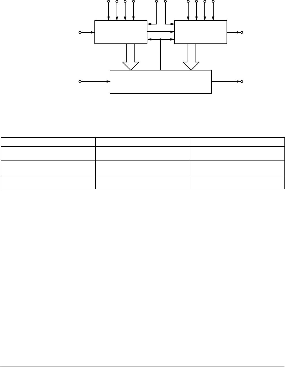
BLOCK DIAGRAM
CTL = Low for Binary Count
CTL = High for BCD Count
CASCADE
FEEDBACK
CLOCK
9
7
V
DD
= PIN 16
V
SS
= PIN 8
15
1
ZERO
DETECT
Q
CLOCK
LOAD
ZERO DETECT ENCODER
BINARY/BCD
COUNTER #1
BINARY/BCD
COUNTER #2
P0 P1 P2 P3 CTL
1
CTL
2
P4 P5 P6 P7
141312
111026
543
ORDERING INFORMATION
Device Package Shipping
MC14569BDWG SOIC−16 WB
(Pb−Free)
47 Units / Rail
MC14569BDWR2G SOIC−16 WB
(Pb−Free)
1000 Units / Tape & Reel
NLV14569BDWR2G* SOIC−16 WB
(Pb−Free)
1000 Units / Tape & Reel
For information on tape and reel specifications, including part orientation and tape sizes, please refer to our Tape and Reel Packaging
Specifications Brochure, BRD8011/D.
*NLV Prefix for Automotive and Other Applications Requiring Unique Site and Control Change Requirements; AEC−Q100 Qualified and PPAP
Capable.
MC14569B
http://onsemi.com
3
ELECTRICAL CHARACTERISTICS (Voltages Referenced to V
SS
)
Characteristic
Symbo
l
V
DD
Vdc
– 55_C 25_C 125_C
Unit
Min Max Min
Typ
(Note 2)
Max Min Max
Output Voltage “0” Level
V
in
= V
DD
or 0
V
OL
5.0
10
15
0.05
0.05
0.05
0
0
0
0.05
0.05
0.05
0.05
0.05
0.05
Vdc
V
in
= 0 or V
DD
“1” Level V
OH
5.0
10
15
4.95
9.95
14.95
4.95
9.95
14.95
5.0
10
15
4.95
9.95
14.95
Vdc
Input Voltage “0” Level
(V
O
= 4.5 or 0.5 Vdc)
(V
O
= 9.0 or 1.0 Vdc)
(V
O
= 13.5 or 1.5 Vdc)
V
IL
5.0
10
15
1.5
3.0
4.0
2.25
4.50
6.75
1.5
3.0
4.0
1.5
3.0
4.0
Vdc
(V
O
= 0.5 or 4.5 Vdc) “1” Level
(V
O
= 1.0 or 9.0 Vdc)
(V
O
= 1.5 or 13.5 Vdc)
V
IH
5.0
10
15
3.5
7.0
11
3.5
7.0
11
2.75
5.50
8.25
3.5
7.0
11
Vdc
Output Drive Current
(V
OH
= 2.5 Vdc) Source
(V
OH
= 4.6 Vdc)
(V
OH
= 9.5 Vdc)
(V
OH
= 13.5 Vdc)
I
OH
5.0
5.0
10
15
–3.0
–0.64
–1.6
–4.2
–2.4
–0.51
–1.3
–3.4
–4.2
–0.88
–2.25
–8.8
–1.7
–0.36
–0.9
–2.4
mAdc
(V
OL
= 0.4 Vdc) Sink
(V
OL
= 0.5 Vdc)
(V
OL
= 1.5 Vdc)
I
OL
5.0
10
15
0.64
1.6
4.2
0.51
1.3
3.4
0.88
2.25
8.8
0.36
0.9
2.4
mAdc
Input Current I
in
15 ±0.1 ±0.00001 ±0.1 ±1.0
mAdc
Input Capacitance
(V
in
= 0)
C
in
5.0 7.5 pF
Quiescent Current
(Per Package)
I
DD
5.0
10
15
5.0
10
20
0.005
0.010
0.015
5.0
10
20
150
300
600
mAdc
Total Supply Current (Notes 3 & 4)
(Dynamic plus Quiescent,
Per Package)
(C
L
= 50 pF on all outputs, all
buffers switching)
I
T
5.0
10
15
I
T
= (0.58 mA/kHz) f + I
DD
I
T
= (1.20 mA/kHz) f + I
DD
I
T
= (1.95 mA/kHz) f + I
DD
mAdc
Product parametric performance is indicated in the Electrical Characteristics for the listed test conditions, unless otherwise noted. Product
performance may not be indicated by the Electrical Characteristics if operated under different conditions.
2. Data labelled “Typ” is not to be used for design purposes but is intended as an indication of the IC’s potential performance.
3. The formulas given are for the typical characteristics only at 25_C.
4. To calculate total supply current at loads other than 50 pF:
I
T
(C
L
) = I
T
(50 pF) + (C
L
– 50) Vfk
where: I
T
is in mA (per package), C
L
in pF, V = (V
DD
– V
SS
) in volts, f in kHz is input frequency, and k = 0.001.

NLV14569BDWR2G

Mfr. #:
Manufacturer:
ON Semiconductor
Description:
Multipliers / Dividers PROGRAMMABLE DIVIDE-
Lifecycle:
New from this manufacturer.
Delivery:
DHL FedEx Ups TNT EMS
Payment:
T/T Paypal Visa MoneyGram Western Union