MC14569B
http://onsemi.com
5
PIN DESCRIPTIONS
INPUTS
P0, P1, P2, P3 (Pins 3, 4, 5, 6) − Preset Inputs.
Programmable inputs for the least significant counter. May
be binary or BCD depending on the control input.
P4, P5, P6, P7 (Pins 11, 12, 13, 14) − Preset Inputs.
Programmable inputs for the most significant counter. May
be binary or BCD depending on the control input.
Clock (Pin 9) − Preset data is decremented by one on each
positive transition of this signal.
OUTPUTS
Zero Detect (Pin 1) − This output is normally low and
goes high for one clock cycle when the counter has
decremented to zero.
Q (Pin 15) − Output of the last stage of the most significant
counter. This output will be inactive unless the preset input
P7 has been set high.
CONTROLS
Cascade Feedback (Pin 7) − This pin is normally set
high. When low, loading of the preset inputs (P0 through P7)
is inhibited, i.e., P0 through P7 are “don’t cares.” Refer to
Table 1 for output characteristics.
CTL
1
(Pin 2) − This pin controls the counting mode of the
least significant counter. When set high, counting mode is
BCD. When set low, counting mode is binary.
CTL
2
(Pin 10) − This pin controls the counting mode of
the most significant counter. When set high, counting mode
is BCD. When set low, counting mode is binary.
SUPPLY PINS
V
SS
(Pin 18) − Negative Supply Voltage. This pin is
usually connected to ground.
V
DD
(Pin 16) − Positive Supply Voltage. This pin is
connected to a positive supply voltage ranging from 3.0 V
to 18 V.
OPERATING CHARACTERISTICS
The MC14569B is a programmable divide−by−N dual
4−bit down counter. This counter may be programmed (i.e.,
preset) in BCD or binary code through inputs P0 to P7. For
each counter, the counting sequence may be chosen
independently by applying a high (for BCD count) or a low
(for binary count) to the control inputs CTL
1
and CTL
2
.
The divide ratio N (N being the value programmed on the
preset inputs P0 to P7) is automatically loaded into the
counter as soon as the count 1 is detected. Therefore, a
division ratio of one is not possible. After N clock cycles,
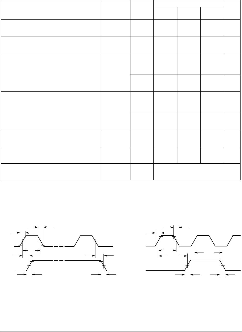
one pulse appears on the Zero Detect output. (See Timing
Diagram.) The Q output is the output of the last stage of the
most significant counter (See Tables 1 through 5, Mode
Controls.)
When cascading the MC14569B to the MC14526B, the
Cascade Feedback input, Q, and Zero Detect outputs must
be respectively connected to “0”, Clock, and Load of the
following counter. If the MC14569B is used alone, Cascade
Feedback must be connected to V
DD
.
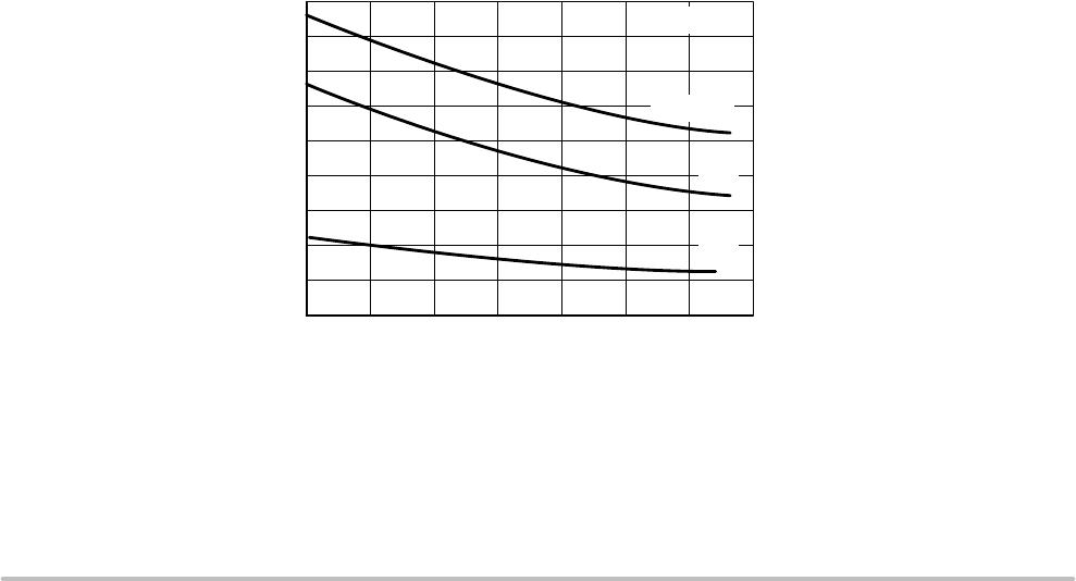
18
16
14
12
10
8.0
6.0
4.0
2.0
0
+ 100+80+60+40+200-20-40
T
A
, AMBIENT TEMPERATURE (°C)
f, FREQUENCY (MHz), TYPICAL
C
L
= 50 pF
V
DD
= 15 V
10 V
5.0 V