© Semiconductor Components Industries, LLC, 2011
June, 2011 Rev. 6
1 Publication Order Number:
CAT9554/D
CAT9554, CAT9554A
8-bit I
2
C and SMBus I/O Port
with Interrupt
Description
The CAT9554 and CAT9554A are CMOS devices that provide 8bit
parallel input/output port expansion for I
2
C and SMBus compatible
applications. These I/O expanders provide a simple solution in
applications where additional I/Os are needed: sensors, power
switches, LEDs, pushbuttons, and fans.
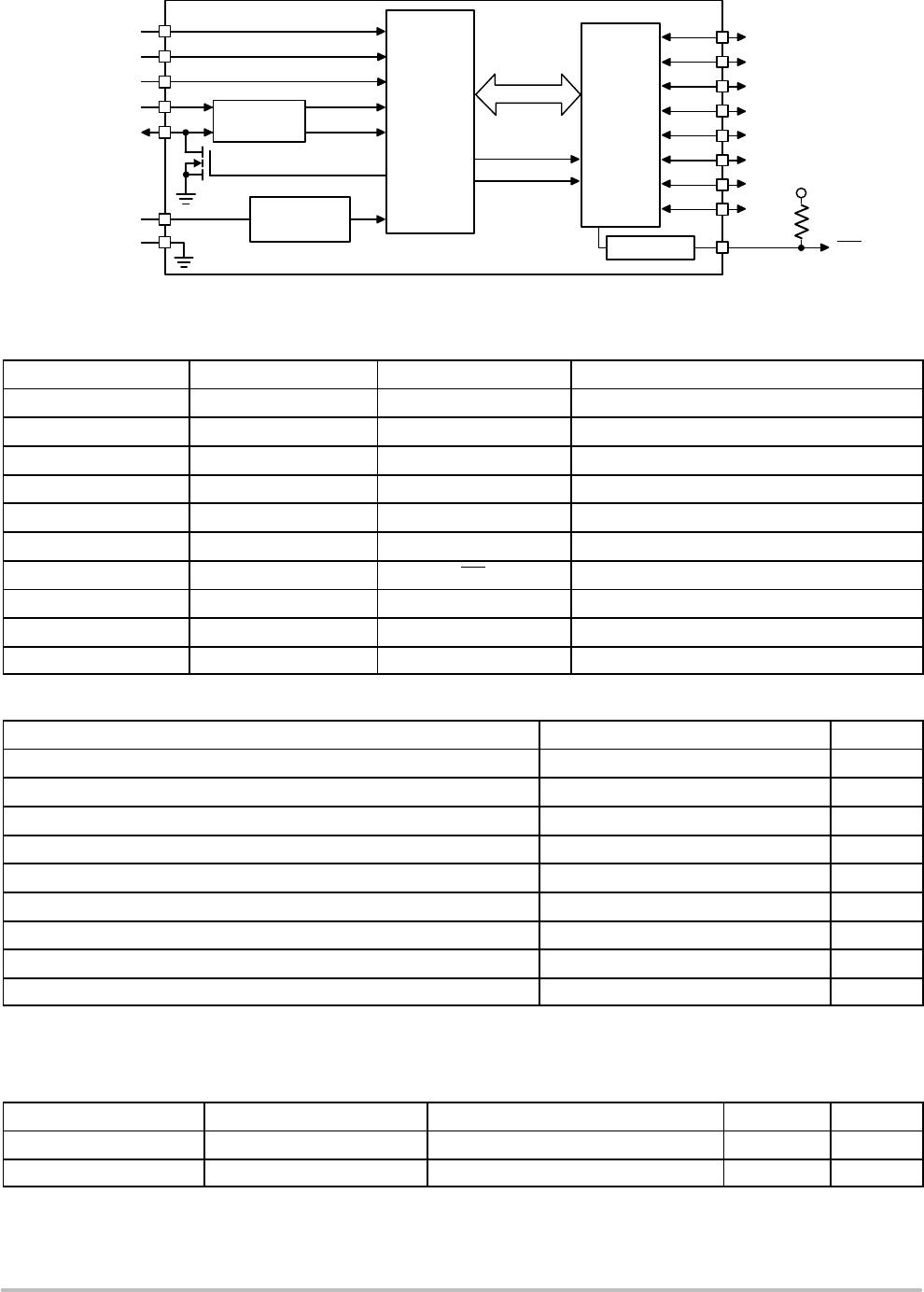
The CAT9554/9554A consist of an input port register, an output port
register, a configuration register, a polarity inversion register and an
I
2
C/SMBuscompatible serial interface.
Any of the eight I/Os can be configured as an input or output by
writing to the configuration register. The system master can invert the
CAT9554/9554A input data by writing to the activehigh polarity
inversion register.
The CAT9554/9554A features an active low interrupt output which
indicates to the system master that an input state has changed.
The device’s extended addressing capability allows up to 8 devices
to share the same bus. The CAT9554A is identical to the CAT9554
except the fixed part of the I
2
C slave address is different. This allows
up to 16 of devices (eight CAT9554 and eight CAT9554A) to be
connected on the same bus.
Features
400 kHz I
2
C Bus Compatible (Note 1)
2.3 V to 5.5 V Operation
Low Standby Current
5 V Tolerant I/Os
8 I/O Pins that Default to Inputs at Powerup
High Drive Capability
Individual I/O Configuration
Polarity Inversion Register
Active Low Interrupt Output
Internal Poweron Reset
No Glitch on Powerup
Noise Filter on SDA/SCL Inputs
Cascadable up to 8 Devices
Industrial Temperature Range
16lead SOIC and TSSOP, and 16pad TQFN (4 x 4 mm) Packages
These Devices are PbFree, Halogen Free/BFR Free and are RoHS
Compliant
Applications
White Goods (dishwashers, washing machines)
Handheld Devices (cell phones, PDAs, digital cameras)
Data Communications (routers, hubs and servers)
1. All I/Os are set to inputs at RESET.
TQFN16
HV4 SUFFIX
CASE 510AE
http://onsemi.com
SOIC16
W SUFFIX
CASE 751BG
PIN CONNECTIONS
SOIC (W), TSSOP (Y)
(Top View)
1
A0
A1
A2
I/O
1
I/O
0
V
CC
SDA
SCL
INT
I/O
7
I/O
6
I/O
5
I/O
4
I/O
2
I/O
3
V
SS
TSSOP16
Y SUFFIX
CASE 948AN
See detailed ordering and shipping information in the package
dimensions section on page 14 of this data sheet.
ORDERING INFORMATION
TQFN 4 x 4 mm (HV4)
(Top View)
SCL
INT
I/O
7
I/O
6
A2
I/O
1
I/O
0
I/O
2
A1
A0
V
CC
SDA
I/O
3
I/O
4
V
SS
I/O
5
1
CAT9554, CAT9554A
http://onsemi.com
2
Figure 1. Block Diagram
8BIT
WRITE pulse
READ pulse
LP FILTER
POWERON
RESET
INPUT
FILTER
CONTROL
A0
A1
A2
SDA
SCL
INPUT/
OUTPUT
PORTS
INT
V
CC
I/O
0
I/O
1
I/O
2
I/O
3
I/O
4
I/O
5
I/O
6
I/O
7
I
2
C/SMBUS
V
CC
V
SS
Note: All I/Os are set to inputs at RESET.
Table 1. PIN DESCRIPTION
SOIC / TSSOP TQFN Pin Name Function
1 15 A0 Address Input 0
2 16 A1 Address Input 1
3 1 A2 Address Input 2
47 25 I/O
03
Input/Output Port 0 to Input/Output Port 3
8 6 V
SS
Ground
912 710 I/O
47
Input/Output Port 4 to Input/Output Port 7
13 11 INT Interrupt Output (open drain)
14 12 SCL Serial Clock
15 13 SDA Serial Data
16 14 V
CC
Power Supply
Table 2. ABSOLUTE MAXIMUM RATINGS
Parameters Ratings Units
V
CC
with Respect to Ground 0.5 to +6.5 V
Voltage on Any Pin with Respect to Ground 0.5 to +5.5 V
DC Current on I/O
0
to I/O
7
±50 mA
DC Input Current ±20 mA
V
CC
Supply Current 85 mA
V
SS
Supply Current 100 mA
Package Power Dissipation Capability (T
A
= 25°C) 1.0 W
Junction Temperature +150 °C
Storage Temperature 65 to +150 °C
Stresses exceeding Maximum Ratings may damage the device. Maximum Ratings are stress ratings only. Functional operation above the
Recommended Operating Conditions is not implied. Extended exposure to stresses above the Recommended Operating Conditions may affect
device reliability.
Table 3. RELIABILITY CHARACTERISTICS
Symbol Parameter Reference Test Method Min Units
V
ZAP
(Note 2) ESD Susceptibility JEDEC Standard JESD 22 2000 Volts
I
LTH
(Notes 2, 3) Latchup JEDEC Standard 17 100 mA
2. This parameter is tested initially and after a design or process change that affects the parameter.
3. Latchup protection is provided for stresses up to 100 mA on address and data pins from 1 V to V
CC
+1 V.
CAT9554, CAT9554A
http://onsemi.com
3
Table 4. D.C. OPERATING CHARACTERISTICS (V
CC
= 2.3 to 5.5 V; T
A
= 40°C to +85°C, unless otherwise specified.)
Symbol
Parameter Conditions Min Typ Max Unit
SUPPLIES
V
CC
Supply voltage 2.3 5.5 V
I
CC
Supply current Operating mode; V
CC
= 5.5 V;
no load; f
SCL
= 100 kHz
104 175
mA
I
stbl
Standby current Standby mode; V
CC
= 5.5 V; no load;
V
I
= V
SS
; f
SCL
= 0 kHz; I/O = inputs
550 700
mA
I
stbh
Standby current Standby mode; V
CC
= 5.5 V; no load;
V
I
= V
CC
; f
SCL
= 0 kHz; I/O = inputs
0.25 1
mA
V
POR
Poweron reset voltage No load; V
I
= V
CC
or V
SS
1.5 1.65 V
SCL, SDA, INT
V
IL
(Note 4) Low level input voltage 0.5 0.3 x V
CC
V
V
IH
(Note 4) High level input voltage 0.7 x V
CC
5.5 V
I
OL
Low level output current V
OL
= 0.4 V 3 mA
I
L
Leakage current V
I
= V
CC
or V
SS
1 +1
mA
C
I
(Note 5) Input capacitance V
I
= V
SS
6 pF
C
O
(Note 5) Output capacitance V
O
= V
SS
8 pF
A0, A1, A2
V
IL
(Note 4) Low level input voltage 0.5 0.8 V
V
IH
(Note 4) High level input voltage 2.0 5.5 V
I
LI
Input leakage current 1 1
mA
I/Os
V
IL
Low level input voltage 0.5 0.8 V
V
IH
High level input voltage 2.0 5.5 V
I
OL
Low level output current
V
OL
= 0.5 V; V
CC
= 2.3 V (Note 6) 8 10 mA
V
OL
= 0.7 V; V
CC
= 2.3 V (Note 6) 10 13 mA
V
OL
= 0.5 V; V
CC
= 4.5 V (Note 6) 8 17 mA
V
OL
= 0.7 V; V
CC
= 4.5 V (Note 6) 10 24 mA
V
OL
= 0.5 V; V
CC
= 3.0 V (Note 6) 8 14 mA
V
OL
= 0.7 V; V
CC
= 3.0 V (Note 6) 10 19 mA
V
OH
High level output
voltage
I
OH
= 8 mA; V
CC
= 2.3 V (Note 7) 1.8 V
I
OH
= 10 mA; V
CC
= 2.3 V (Note 7) 1.7 V
I
OH
= 8 mA; V
CC
= 3.0 V (Note 7) 2.6 V
I
OH
= 10 mA; V
CC
= 3.0 V (Note 7) 2.5 V
I
OH
= 8 mA; V
CC
= 4.75 V (Note 7) 4.1 V
I
OH
= 10 mA; V
CC
= 4.75 V (Note 7) 4.0 V
I
IH
Input leakage current V
CC
= 3.6 V; V
I
= V
CC
1
mA
I
IL
Input leakage current V
CC
= 5.5 V; V
I
= V
SS
100
mA
C
I
(Note 5) Input capacitance 5 pF
C
O
(Note 5) Output capacitance 8 pF
4. V
IL
min
and V
IH
max
are reference values only and are not tested.
5. This parameter is characterized initially and after a design or process change that affects the parameter. Not 100% tested.
6. The total current sunk by all I/Os must be limited to 100 mA and each I/O limited to 25 mA maximum.
7. The total current sourced by all I/Os must be limited to 85 mA.

CAT9554AWI-GT2

Mfr. #:
Manufacturer:
ON Semiconductor
Description:
Interface - I/O Expanders I2C/SMBUS Expander 8B,w/Int
Lifecycle:
New from this manufacturer.
Delivery:
DHL FedEx Ups TNT EMS
Payment:
T/T Paypal Visa MoneyGram Western Union