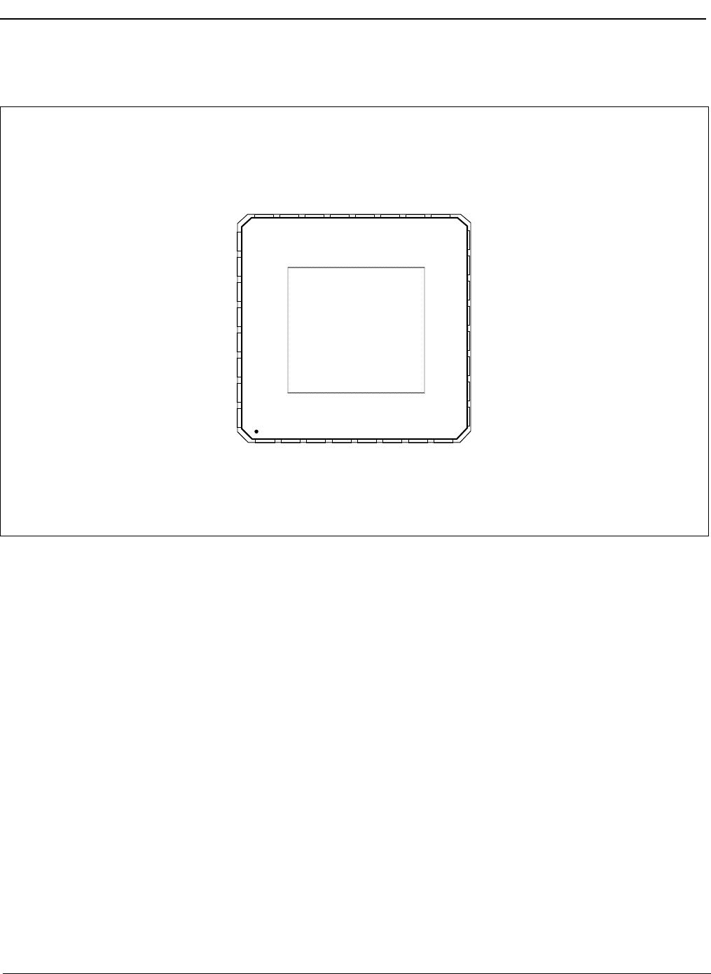
ZL40217 Data Sheet
6
Microsemi Corporation
3.0 Functional Description
he ZL40217 is an LVDS clock fanout buffer with six output clock drivers capable of operating at frequencies up to
750MHz.
The ZL40217 provides an internal input termination netwo
rk for DC and AC coupled inputs; optional input biasing
for AC coupled inputs is also provided. The ZL40217 can accept DC or AC coupled LVPECL and LVDS input
signals, AC coupled CML or HCSL input signals, and single ended signals. A pin compatible device with external
termination is also available.
The ZL40217 is designed to fan out
low-jitter reference clocks for wired or optical communications applications
while adding minimal jitter to the clock signal. An internal linear power supply regulator and bulk capacitors
minimize additive jitter due to power supply noise. The device operates from 2.5V+/-5% or 3.3V+/-5% supply. Its
operation is guaranteed over the industrial temperature range -40°C to +85°C.
The device block diagram is shown in Figure 1; its operation is described in the following sections.
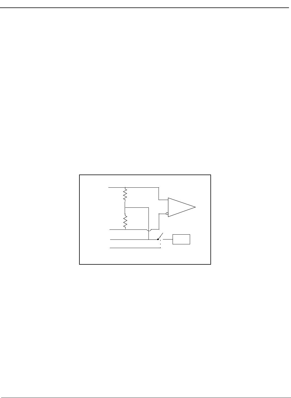
3.1 Clock Inputs
The device has a differential input equipped with two on-chip 50 Ohm termination resistors arranged in series with a
center tap. The input can accept many differential and single-ended signals with AC or DC coupling as appropriate.
A control pin is available to enable internal biasing for AC coupled inputs. A block diagram of the input stage is in
Figure 3.
Receiver
clk_n
50
clk_p
Vt
50
Bias
ctrl
Figure 3 - Simplified Diagram of input stage
This following figures give the components values and configu
ration for the various circuits compatible with the
input stage and the use of the Vt and ctrl pins in each case.
In the following diagrams were the ct
rl pin is "1" and the Vt pin is not connected, the Vt pin can be instead
connected to V
DD
with a capacitor. A capacitor can also help in Figure 4 between Vt and V
DD
. This capacitor will
minimize the noise at the point between the two inter
nal termination resistors and improve the overall performance
of the device.