Data Sheet HMC1131
Rev. A | Page 3 of 14
ELECTRICAL SPECIFICATIONS
24 GHz TO 27 GHz FREQUENCY RANGE
T
A
= 25°C, V
DD
1 = V
DD
2 = V
DD
3 = V
DD
4 = 5 V, I
DD
= 225 mA, unless otherwise stated. Adjust V
GG
1 and V
GG
2 between −2 V to 0 V to
achieve I
DD
= 225 mA typical.
Table 1.
Parameter Symbol Min Typ Max Unit
FREQUENCY RANGE 24 27 GHz
GAIN 18 22 dB
Gain Variation Over Temperature 0.031 dB/°C
RETURN LOSS
Input 8 dB
Output 7 dB
OUTPUT
Output Power for 1 dB Compression P1dB 20 23 dBm
Saturated Output Power P
SAT
27 dBm
Output Third-Order Intercept
1
IP3 34 dBm
SUPPLY CURRENT
Total Supply Current I
DD
225 mA
Total Supply Current vs. V
DD
2
4 V
5 V
1
Measurement taken at P
OUT
/tone = 10 dBm.
2
The amplifier operates over the full voltage ranges shown. V
GG
1 and V
GG
2 are adjusted to achieve I
DD
= 225 mA at 5 V.
27 GHz TO 35 GHz FREQUENCY RANGE
T
A
= 25°C, V
DD
1 = V
DD
2 = V
DD
3 = V
DD
4 = 5 V, I
DD
= 225 mA, unless otherwise stated. Adjust V
GG
1 and V
GG
2 between −2 V to 0 V to
achieve I
DD
= 225 mA typical.
Table 2.
Parameter Symbol Min Typ Max Unit
FREQUENCY RANGE 27 35 GHz
GAIN 18 20 dB
Gain Variation Over Temperature 0.031 dB/°C
RETURN LOSS
Input 8 dB
Output 7 dB
OUTPUT
Output Power for 1 dB Compression P1dB 21 24 dBm
Saturated Output Power P
SAT
25 dBm
Output Third-Order Intercept
1
IP3 35 dBm
SUPPLY CURRENT
Total Supply Current I
DD
225 mA
Total Supply Current vs. V
DD
2
4 V
5 V
1
Measurement taken at P
OUT
/tone = 10 dBm.
2
The amplifier operates over the full voltage ranges shown. V
GG
1 and V
GG
2 are adjusted to achieve I
DD
= 225 mA at 5 V.
HMC1131 Data Sheet
Rev. A | Page 4 of 14
ABSOLUTE MAXIMUM RATINGS
Table 3.
Parameter Rating
Drain Bias Voltage (V
DD
) 5.5 V
RF Input Power (RFIN) 12 dBm
Channel Temperature 175°C
Continuous Power Dissipation (P
DISS
),
T
A
= 85°C (Derate 22 mW/°C)
1.97 W
Thermal Resistance, R
TH
(Junction to
Ground Paddle)
45.5°C/W
Operating Temperature 40°C to +85°C
Storage Temperature 65°C to +150°C
ESD Sensitivity, Human Body Model (HBM) Class 0,
passed 150 V
Maximum Peak Reflow Temperature 260°C
Stresses at or above those listed under Absolute Maximum
Ratings may cause permanent damage to the product. This is a
stress rating only; functional operation of the product at these
or any other conditions above those indicated in the operational
section of this specification is not implied. Operation beyond
the maximum operating conditions for extended periods may
affect product reliability.
ESD CAUTION
Data Sheet HMC1131
Rev. A | Page 5 of 14
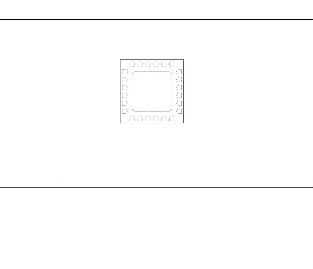
PIN CONFIGURATION AND FUNCTION DESCRIPTIONS
1
NIC
2
GND
3
RFIN
4
GND
5
NIC
6
NIC
18
NIC
17
GND
16
RFOUT
15
GND
14
NIC
13
NIC
24
NIC
23
V
DD
1
22
V
DD
2
21
V
DD
3
20
V
DD
4
19
NIC
7
NIC
8
V
GG
1
9
NIC
10
NIC
11
V
GG
2
12
NIC
HMC1131
TOP VIEW
(Not to Scale)
NOTES
1. NIC = NOT INTERNALLY CONNECTED.
2. THE EXPOSED PAD MUST BE CONNECTED
TO RF/DC GROUND.
13105-100
Figure 2. Pin Configuration
Table 4. Pin Function Descriptions
Pin No. Mnemonic Description
1, 5 to 7, 9, 10, 12 to 14,
18, 19, 24
NIC
Not Internally Connected. However, all data was measured with these pins connected to RF/dc
ground externally.
2, 4, 15, 17 GND Ground. These pins must be connected to RF/dc ground.
3 RFIN RF Input. This pin is ac-coupled and matched to 50 Ω.
8 V
GG
1
Gate Bias Pin for the First and Second Stages. External bypass capacitors of 100 pF, 10 nF, and 4.7 μF
are required for this pin.
11 V
GG
2
Gate Bias Pin for the Third and Fourth Stages. External bypass capacitors of 100 pF, 10 nF, and 4.7 μF
are required for this pin.
16 RFOUT RF Output. This pin is ac-coupled and matched to 50 Ω.
20 to 23 V
DD
4 to V
DD
1
Drain Bias Voltage Pins. External bypass capacitors of 100 pF, 10 nF, and 4.7 μF are required for
these pins.
EPAD Exposed Pad. The exposed pad must be connected to RF/dc ground.

EV1HMC1131LC4

Mfr. #:
Manufacturer:
Analog Devices Inc.
Description:
EVAL BOARD FOR HMC1131
Lifecycle:
New from this manufacturer.
Delivery:
DHL FedEx Ups TNT EMS
Payment:
T/T Paypal Visa MoneyGram Western Union

Products related to this Datasheet