7©2018 Integrated Device Technology, Inc. May 30, 2018
9FGV1005 Datasheet
Table 7. LVCMOS Output Electrical Characteristics
Parameter Symbol Conditions Minimum Typical Maximum Units
Slew Rate S
R
3.3V ±5%, 20% to 80% of V
DDO
(output
load = 4.7pF).
2.5 3.7 4.6
V/ns
2.5V ±5%, 20% to 80% of V
DDO
(output
load = 4.7pF).
1.5 2.4 4.6
1.8V ±5%, 20% to 80% of V
DDO
(output
load = 4.7pF).
0.8 1.7 3.5
Output High Voltage V
OH
I
OH
= -15mA at 3.3V.
0.8 x V
DDO
V
DDO
VI
OH
= -12mA at 2.5V.
I
OH
= -8mA at 1.8V.
Output Low Voltage V
OL
I
OL
= 15mA at 3.3V.
0.22 0.4 VI
OL
= 12mA at 2.5V.
I
OL
= 8mA at 1.8V.
Output Leakage Current
(OUT[0:1])
I
OZDD
Programmable outputs, tri-state, V
DDO
= 3.465V.
05μA
Output Leakage Current (REF) I
OZDD
REF outputs, tri-state, V
DDO
= 3.465V. 0 5 μA
CMOS Output Driver Impedance R
OUT
T
A
= 25°C. 17
Table 8. LVDS Output Electrical Characteristics
Parameter Symbol Minimum Typical Maximum Units
Differential Output Voltage for the TRUE Binary State V
OT
(+) 247 328 454 mV
Differential Output Voltage for the FALSE Binary State V
OT
(-) -454 -332 -247 mV
Change in V
OT
between Complementary Output States ΔV
OT
50 mV
Output Common Mode Voltage (Offset Voltage) at 3.3V +5% & 2.5V +5% V
OS
1.125 1.19 1.55 V
Output Common Mode Voltage (Offset Voltage) at 1.8V +5% V
OS
0.8 0.86 0.95 V
Change in V
OS
between Complementary Output States ΔV
OS
050mV
Outputs Short Circuit Current, V
OUT
+ or V
OUT
- = 0V or V
DD
I
OS
612mA
Differential Outputs Short Circuit Current, V
OUT
+ = V
OUT
-I
OSD
312mA
Rise Times Tested at 20% – 80% T
R
257 400 ps
Fall Times Tested at 80% – 20% T
F
287 400 ps
8©2018 Integrated Device Technology, Inc. May 30, 2018
9FGV1005 Datasheet
1
Measured from single-ended waveform.
2
Measured from differential waveform.
3
Measured from -150mV to +150mV on the differential waveform (derived from REFCLK+ minus REFCLK-). The signal must be monotonic through
the measurement region for rise and fall time. The 300mV measurement window is centered on the differential zero crossing.
4
Measured at crossing point where the instantaneous voltage value of the rising edge of REFCLK+ equals the falling edge of REFCLK-.
5
Refers to the total variation from the lowest crossing point to the highest, regardless of which edge is crossing. Refers to all crossing points for this
measurement.
6
Defined as the absolute minimum or maximum instantaneous period. This includes cycle to cycle jitter, relative ppm tolerance, and spread spectrum
modulation.
7
Defined as the maximum instantaneous voltage including overshoot.
8
Defined as the minimum instantaneous voltage including undershoot.
9
Defined as the total variation of all crossing voltages of rising REFCLK+ and falling REFCLK-. This is the maximum allowed variance in V
CROSS
for
any particular system.
10
Refer to section 4.3.7.1.1 of the PCI Express Base Specification, Revision 3.0 for information regarding ppm considerations.
11
System board compliance measurements must use the test load. REFCLK+ and REFCLK- are to be measured at the load capacitors CL. Single
ended probes must be used for measurements requiring single ended measurements. Either single ended probes with math or differential probe
can be used for differential measurements. Test load C
L
= 2pF.
12
T
STABLE
is the time the differential clock must maintain a minimum ±150mV differential voltage after rising/falling edges before it is allowed to droop
back into the VRB ±100mV differential range.
13
“ppm” refers to parts per million and is a DC absolute period accuracy specification. 1 ppm is 1/1,000,000th of 100.000000MHz exactly or 100Hz.
For 300ppm, then we have an error budget of 100Hz/ppm × 300 ppm = 30kHz. The period is to be measured with a frequency counter with
measurement window set to 100ms or greater. The ±300 ppm applies to systems that do not employ spread spectrum clocking, or that use common
clock source. For systems employing spread spectrum clocking, there is an additional 2,500 ppm nominal shift in maximum period resulting from
the 0.5% down spread resulting in a maximum average period specification of +2,800 ppm.
14
Matching applies to rising edge rate for REFCLK+ and falling edge rate for REFCLK-. It is measured using a ±75mV window centered on the median
cross point where REFCLK+ rising meets REFCLK- falling. The median cross point is used to calculate the voltage thresholds the oscilloscope is
to use for the edge rate calculations. The rise edge rate of REFCLK+ should be compared to the fall edge rate of REFCLK-; the maximum allowed
difference should not exceed 20% of the slowest edge rate.
15
At default amplitude settings.
16
Guaranteed by design and characterization.
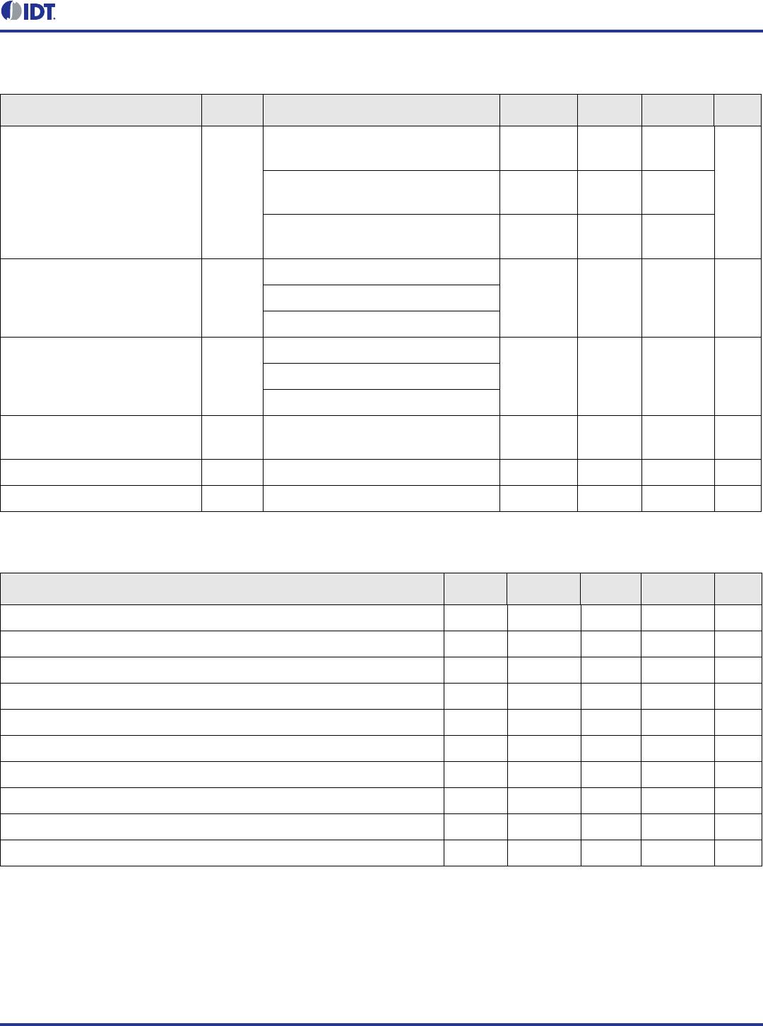
Table 9. Low-Power (LP) Push-Pull HCSL Differential Outputs
V
DDO
= 3.3V ±5%, 2.5V ±5%, 1.8V ±5%, T
A
= -40°C to +85°C unless stated otherwise.
Parameter Symbol Conditions Minimum Typical Maximum Units Notes
Slew Rate T
R/F
Scope averaging on. 1 2.5 4 V/ns 2,3,16
Slew Rate Matching ΔT
R/F
9 20 % 1,14,16
Crossing Voltage (abs) V
CROSS
Scope averaging off. 250 424 550 mV 1,4,5,16
Crossing Voltage (var) ΔV
CROSS
Scope averaging off. 16 140 mV 1,4,9,16
Voltage High V
HIGH
660 785 850 mV 1
Voltage Low V
LOW
-150 13 150 mV 1
Absolute Maximum Voltage V
MAX
808 1150 mV 1,7,15
Absolute Minimum Voltage V
MIN
-300 -54 mV 1,8,15
9©2018 Integrated Device Technology, Inc. May 30, 2018
9FGV1005 Datasheet
Notes for Filtered Phase Jitter Parameters tables:
1
Applies to all differential outputs at 100MHz, guaranteed by design and characterization.
2
Based on PCIe Base Specification Rev4.0 version 0.7draft. See http://www.pcisig.com for latest specifications.
3
Sample size of at least 100K cycles. This figure extrapolates to 108ps pk-pk at 1M cycles for a BER of 1
-12
.
4
IR is the new name for Separate Reference Independent Spread (SRIS) and Separate Reference no Spread (SRNS) PCIe clock architectures.
5
According to the PCIe Base Specification Rev4.0 version 0.7 draft, the jitter transfer functions and corresponding jitter limits are not defined for the
IR clock architecture. Widely accepted industry limits using widely accepted industry filters are used to populate this table. There are no accepted
filters or limits for IR clock architectures at PCIe Gen1 or Gen4 data rates.
Table 10. Filtered Phase Jitter Parameters – PCIe Common Clocked (CC) Architectures
T
AMB
= over the specified operating range. Supply Voltages per normal operation conditions; see Test Loads for loading conditions.
Parameter Symbol Conditions Minimum Typical Maximum
Industry
Limits
Units Notes
PCIe Phase
Jitter
t
jphPCIeG1-CC
PCIe Gen1. 11 18 86
ps
(p-p)
1,2,3
t
jphPCIeG2-CC
PCIe Gen2 Low Band
10kHz < f < 1.5MHz
(PLL BW of 5–16MHz, 8–16MHz,
CDR = 5MHz).
0.1 0.14 3
ps
(rms)
1,2
PCIe Gen2 High Band
1.5MHz < f < Nyquist (50MHz)
(PLL BW of 5–16MHz, 8–16MHz,
CDR = 5MHz).
1.1 1.6 3.1
ps
(rms)
1,2
t
jphPCIeG3-CC
PCIe Gen3
(PLL BW of 2–4MHz, 2–5MHz,
CDR = 10MHz).
0.3 0.39 1
ps
(rms)
1,2
t
jphPCIeG4-CC
PCIe Gen4
(PLL BW of 2–4MHz, 2–5MHz,
CDR = 10MHz).
0.3 0.39 0.5
ps
(rms)
1,2
Table 11. Filtered Phase Jitter Parameters – PCIe Independent Reference (IR) Architectures
T
AMB
= over the specified operating range. Supply Voltages per normal operation conditions; see Test Loads for loading conditions.
Parameter Symbol Conditions Minimum Typical Maximum
Industry
Limits
Units Notes
PCIe
Phase Jitter
t
jphPCIeG2-SRIS
PCIe Gen2
(PLL BW of 16MHz, CDR = 5MHz).
1.0 1.40 2
ps
(rms)
1,4,5
t
jphPCIeG3-SRIS
PCIe Gen3
(PLL BW of 2–4MHz, CDR = 10MHz).
0.3 0.41 0.7
ps
(rms)
1,4,5

9FGV1005A001LTGI

Mfr. #:
Manufacturer:
IDT
Description:
Clock Generators & Support Products 2 O/P 1INT PHI CLOCK
Lifecycle:
New from this manufacturer.
Delivery:
DHL FedEx Ups TNT EMS
Payment:
T/T Paypal Visa MoneyGram Western Union