VS-30TPS16LHM3

VS-30TPS16LHM3
www.vishay.com
Vishay Semiconductors
Revision: 22-Feb-18
1
Document Number: 96491
For technical questions within your region: DiodesAmericas@vishay.com
, DiodesAsia@vishay.com, DiodesEurope@vishay.com
THIS DOCUMENT IS SUBJECT TO CHANGE WITHOUT NOTICE. THE PRODUCTS DESCRIBED HEREIN AND THIS DOCUMENT
ARE SUBJECT TO SPECIFIC DISCLAIMERS, SET FORTH AT www.vishay.com/doc?91000
Thyristor High Voltage, Phase Control SCR, 30 A
FEATURES
AEC-Q101 qualified
Meets JESD 201 class 1A whisker test
Flexible solution for reliable AC power
rectification
Easy control peak current at charger power
up to reduce passive / electromechanical components
Material categorization: for definitions of compliance
please see www.vishay.com/doc?99912
APPLICATIONS
On-board and off-board EV / HEV battery chargers
Renewable energy inverters
DESCRIPTION
The VS-30TPS16LHM3 high voltage series of silicon
controlled rectifiers are specifically designed for medium
power switching and phase control applications.
PRIMARY CHARACTERISTICS
I
T(AV)
20 A
V
DRM
/V
RRM
1600 V
V
TM
1.3 V
I
GT
45 mA
T
J
-40 °C to +125 °C
Package TO-247AD 3L
Circuit configuration Single SCR
(G) 3
2
(A)
1 (K)
TO-247AD 3L
1
2
3
MAJOR RATINGS AND CHARACTERISTICS
PARAMETER TEST CONDITIONS VALUES UNITS
I
T(AV)
Sinusoidal waveform 20
A
I
RMS
30
V
RRM
/V
DRM
1600 V
I
TSM
300 A
V
T
20 A, T
J
= 25 °C 1.3 V
dV/dt 500 V/μs
dI/dt 150 A/μs
T
J
-40 to +125 °C
VOLTAGE RATINGS
PART NUMBER
V
RRM
/V
DRM
, MAXIMUM
REPETITIVE PEAK AND
OFF-STATE VOLTAGE
V
V
RSM
, MAXIMUM
NON-REPETITIVE PEAK
REVERSE VOLTAGE
V
I
RRM
/I
DRM
AT 125 °C
mA
VS-30TPS16LHM3 1600 1700 10
VS-30TPS16LHM3
www.vishay.com
Vishay Semiconductors
Revision: 22-Feb-18
2
Document Number: 96491
For technical questions within your region: DiodesAmericas@vishay.com
, DiodesAsia@vishay.com, DiodesEurope@vishay.com
THIS DOCUMENT IS SUBJECT TO CHANGE WITHOUT NOTICE. THE PRODUCTS DESCRIBED HEREIN AND THIS DOCUMENT
ARE SUBJECT TO SPECIFIC DISCLAIMERS, SET FORTH AT www.vishay.com/doc?91000
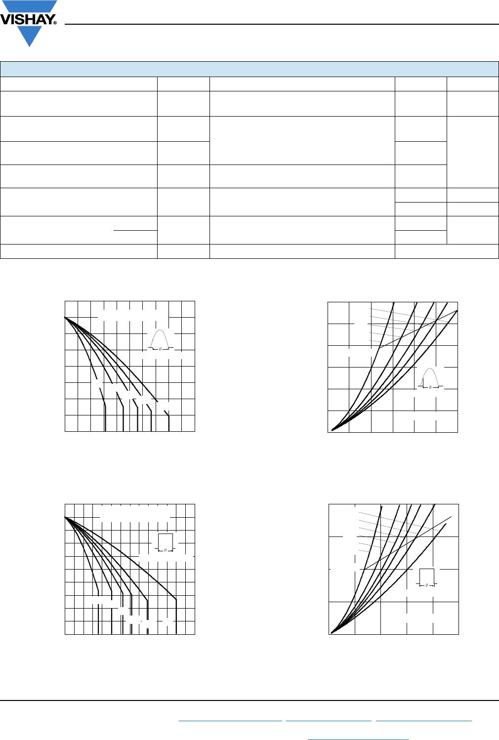
ABSOLUTE MAXIMUM RATINGS
PARAMETER SYMBOL TEST CONDITIONS VALUES UNITS
Maximum average on-state current I
T(AV)
T
C
= 95 °C, 180° conduction half sine wave 20
A
Maximum RMS on-state current I
RMS
30
Maximum peak, one-cycle,
non-repetitive surge current
I
TSM
10 ms sine pulse, rated V
RRM
applied 250
10 ms sine pulse, no voltage reapplied 300
Maximum I
2
t for fusing I
2
t
10 ms sine pulse, rated V
RRM
applied 310
A
2
s
10 ms sine pulse, no voltage reapplied 442
Maximum I
2
t for fusing I
2
t t = 0.1 to 10 ms, no voltage reapplied 4420 A
2
s
Maximum on-state voltage drop V
TM
20 A, T
J
= 25 °C 1.3 V
On-state slope resistance r
t
T
J
= 125 °C
12 m
Threshold voltage V
T(TO)
1.0 V
Maximum reverse and direct leakage current I
RM
/I
DM
T
J
= 25 °C
V
R
= rated V
RRM
/V
DRM
0.5
mA
T
J
= 125 °C 10
Maximum holding current I
H
Anode supply = 6 V, resistive load, initial I
T
= 1 A, T
J
= 25 °C 150
Maximum latching current I
L
Anode supply = 6 V, resistive load, T
J
= 25 °C 200
Maximum rate of rise of off-state voltage dV/dt T
J
= T
J
maximum, linear to 80 % V
DRM
, R
g
- k = open 500 V/µs
Maximum rate of rise of turned-on current dI/dt 150 A/µs
TRIGGERING
PARAMETER SYMBOL TEST CONDITIONS VALUES UNITS
Maximum peak gate power P
GM
8.0
W
Maximum average gate power P
G(AV)
2.0
Maximum peak positive gate current + I
GM
1.5 A
Maximum peak negative gate voltage - V
GM
10 V
Maximum required DC gate current to trigger I
GT
Anode supply = 6 V, resistive load, T
J
= - 10 °C 60
mAAnode supply = 6 V, resistive load, T
J
= 25 °C 45
Anode supply = 6 V, resistive load, T
J
= 125 °C 20
Maximum required DC gate
voltage to trigger
V
GT
Anode supply = 6 V, resistive load, T
J
= - 10 °C 2.5
V
Anode supply = 6 V, resistive load, T
J
= 25 °C 2.0
Anode supply = 6 V, resistive load, T
J
= 125 °C 1.0
Maximum DC gate voltage not to trigger V
GD
T
J
= 125 °C, V
DRM
= rated value
0.25
Maximum DC gate current not to trigger I
GD
2.0 mA
SWITCHING
PARAMETER SYMBOL TEST CONDITIONS VALUES UNITS
Typical turn-on time t
gt
T
J
= 25 °C 0.9
μsTypical reverse recovery time t
rr
T
J
= 125 °C
4
Typical turn-off time t
q
110
VS-30TPS16LHM3
www.vishay.com
Vishay Semiconductors
Revision: 22-Feb-18
3
Document Number: 96491
For technical questions within your region: DiodesAmericas@vishay.com
, DiodesAsia@vishay.com, DiodesEurope@vishay.com
THIS DOCUMENT IS SUBJECT TO CHANGE WITHOUT NOTICE. THE PRODUCTS DESCRIBED HEREIN AND THIS DOCUMENT
ARE SUBJECT TO SPECIFIC DISCLAIMERS, SET FORTH AT www.vishay.com/doc?91000
Fig. 1 - Current Rating Characteristics
Fig. 2 - Current Rating Characteristics
Fig. 3 - On-State Power Loss Characteristics
Fig. 4 - On-State Power Loss Characteristics
THERMAL AND MECHANICAL SPECIFICATIONS
PARAMETER SYMBOL TEST CONDITIONS VALUES UNITS
Maximum junction and storage
temperature range
T
J
, T
Stg
-40 to 125 °C
Maximum thermal resistance,
junction to case
R
thJC
DC operation
0.8
°C/W
Maximum thermal resistance,
junction to ambient
R
thJA
40
Maximum thermal resistance,
case to heatsink
R
thCS
Mounting surface, smooth and greased 0.2
Approximate weight
6g
0.21 oz.
Mounting torque
minimum 6 (5)
kgf · cm
(lbf · in)
maximum 12 (10)
Marking device Case style TO-247AD 3L 30TPS16H
90
100
110
120
130
0 5 10 15 20 25
30°
60°
90°
120°
180°
Maximum Allowable Case Temperature (°C)
Conduction Angle
Average On-state Current (A)
R (DC) = 0.8 °C/W
thJC
80
90
100
110
120
130
0 5 10 15 20 25 30 35
DC
30°
60°
90°
120°
180°
Average On-state Current (A)
Maximum Allowable Case Temperature (°C)
Conduction Period
R (DC) = 0.8 °C/W
thJC
0
10
20
30
40
50
60
0 5 10 15 20 25 30
RMS Limit
Conduction Angle
Maximum Average On-state Power Loss (W)
Average On-state Current (A)
180°
120°
90°
60°
30°
T = 125 °C
J
0
20
40
60
80
0 10 20 30 40 50
DC
180°
120°
90°
60°
30°
RMS limit
Conduction period
Maximum Average On-state Power Loss (W)
Average On-state Current (A)
T = 125 °C
J

VS-30TPS16LHM3

Mfr. #:
Manufacturer:
Vishay Semiconductors
Description:
SCRs 20A If; 1600V Vr TO-247AD 3L
Lifecycle:
New from this manufacturer.
Delivery:
DHL FedEx Ups TNT EMS
Payment:
T/T Paypal Visa MoneyGram Western Union

Products related to this Datasheet