74LCX541FT
1
CMOS Digital Integrated Circuits Silicon Monolithic
74LCX541FT
74LCX541FT
74LCX541FT
74LCX541FT
Start of commercial production
2013-10
1.
1.
1.
1. Functional Description
Functional Description
Functional Description
Functional Description
• Low-Voltage Octal Bus Buffer with 5-V Tolerant Inputs and Outputs
2.
2.
2.
2. General
General
General
General
The 74LCX541FT is a high-performance CMOS octal bus buffer. Designed for use in 3.3-V systems, it achieves
high-speed operation while maintaining the CMOS low power dissipation.
The device is designed for low-voltage (3.3 V) V
CC
applications, but it could be used to interface to 5 V supply
environment for both inputs and outputs.
The 74LCX541FT is a non-inverting 3-state buffer having two active-low output enables. When either OE1 or OE2
are high, the terminal outputs are in the high-impedance state. This device is designed to be used with 3-state
memory address drivers, etc.
All inputs are equipped with protection circuits against static discharge.
3.
3.
3.
3. Features
Features
Features
Features
(1) Low-voltage operation: V
CC
= 1.65 to 3.6 V
(2) High-speed operation: t
pd
= 6.5 ns (max) (V
CC
= 3.0 to 3.6 V)
(3) Output current: |I
OH
|/I
OL
= 24 mA (min) (V
CC
= 3.0 to 3.6 V)
(4) Power-down protection provided on all inputs and outputs
(5) Pin and function compatible with the 74 series
(74LVC/ALVC/ etc.) 541 type
4.
4.
4.
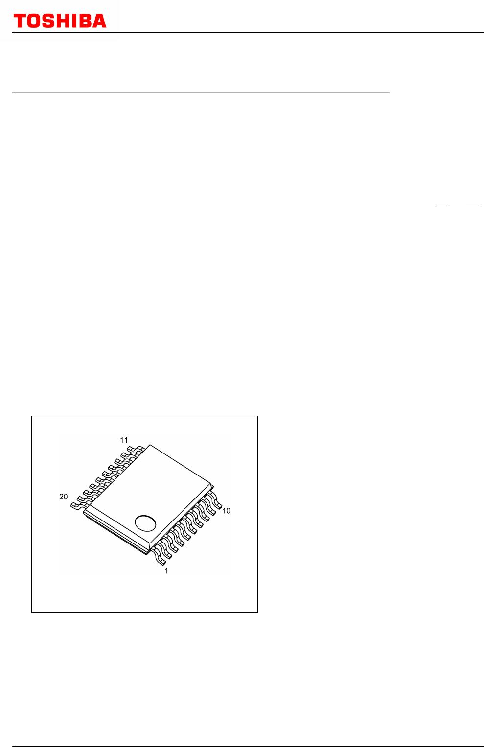
4. Packaging
Packaging
Packaging
Packaging
2014-06-24
Rev.2.0