74LCX541FT
5
11.2.
11.2.
11.2.
11.2. AC Characteristics (Unless otherwise specified, T
AC Characteristics (Unless otherwise specified, T
AC Characteristics (Unless otherwise specified, T
AC Characteristics (Unless otherwise specified, T
a
a
a
a
= -40 to 85
= -40 to 85
= -40 to 85
= -40 to 85
)
)
)
)
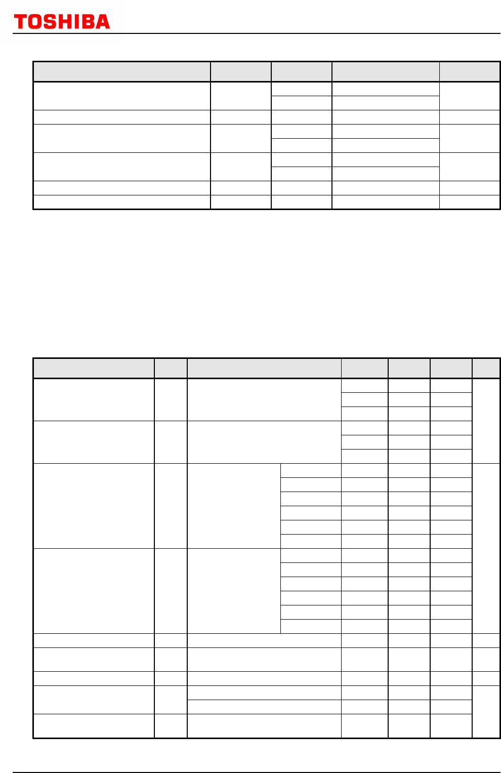
Characteristics
Propagation delay time
3-state output enable time
3-state output disable time
Output skew
Symbol
t
PLH
,t
PHL
t
PZL
,t
PZH
t
PLZ
,t
PHZ
t
osLH
,t
osHL
Note
(Note 1)
Test Condition
See 11.5 AC Test Circuit,
Table 11.5.1, Fig. 11.6.1
See 11.5 AC Test Circuit,
Table 11.5.1, Fig. 11.6.2
See 11.5 AC Test Circuit,
Table 11.5.1, Fig. 11.6.2
V
CC
(V)
1.8 ± 0.15
2.5 ± 0.2
2.7
3.3 ± 0.3
1.8 ± 0.15
2.5 ± 0.2
2.7
3.3 ± 0.3
1.8 ± 0.15
2.5 ± 0.2
2.7
3.3 ± 0.3
2.7
3.3 ± 0.3
Min
1.5
1.5
1.5
Max
25.0
8.5
7.5
6.5
34.0
17.0
9.5
8.5
32.0
16.0
8.5
7.5
1.0
Unit
ns
ns
ns
ns
Note 1: Parameter guaranteed by design. (t
osLH
= |t
PLHm
- t
PLHn
|, t
osHL
= |t
PHLm
- t
PHLn
|)
11.3.
11.3.
11.3.
11.3. Dynamic Switching Characteristics (Unless otherwise specified, T
Dynamic Switching Characteristics (Unless otherwise specified, T
Dynamic Switching Characteristics (Unless otherwise specified, T
Dynamic Switching Characteristics (Unless otherwise specified, T
a
a
a
a
= 25
= 25
= 25
= 25
, Input: t
, Input: t
, Input: t
, Input: t
r
r
r
r
= t
= t
= t
= t
f
f
f
f
= 2.5 ns, C
= 2.5 ns, C
= 2.5 ns, C
= 2.5 ns, C
L
L
L
L
= 50 pF, R
= 50 pF, R
= 50 pF, R
= 50 pF, R
L
L
L
L
= 500
= 500
= 500
= 500 Ω
Ω
Ω
Ω)
)
)
)
Characteristics
Quiet output maximum dynamic V
OL
Quiet output minimum dynamic V
OL
Symbol
V
OLP
|V
OLV
|
Test Condition
V
IH
= 3.3 V, V
IL
= 0 V
V
IH
= 3.3 V, V
IL
= 0 V
V
CC
(V)
3.3
3.3
Typ.
0.8
0.8
Unit
V
V
11.4.
11.4.
11.4.
11.4. Capacitive Characteristics (Unless otherwise specified, T
Capacitive Characteristics (Unless otherwise specified, T
Capacitive Characteristics (Unless otherwise specified, T
Capacitive Characteristics (Unless otherwise specified, T
a
a
a
a
= 25
= 25
= 25
= 25
)
)
)
)
Characteristics
Input capacitance
Output capacitance
Power dissipation capacitance
Symbol
C
IN
C
OUT
C
PD
Note
(Note 1)
Test Condition
f
IN
= 10 MHz
V
CC
(V)
3.3
3.3
3.3
Typ.
7
8
40
Unit
pF
pF
pF
Note 1: C
PD
is defined as the value of the internal equivalent capacitance which is calculated from the operating current
consumption without load. Average operating current can be obtained by the equation.
I
CC(opr)
= C
PD
× V
CC
× f
IN
+ I
CC
/8 (per bit)
2014-06-24
Rev.2.0