DocID031526 Rev 1 13/25
STCH03 Application information
25
6.5 Constant voltage operation
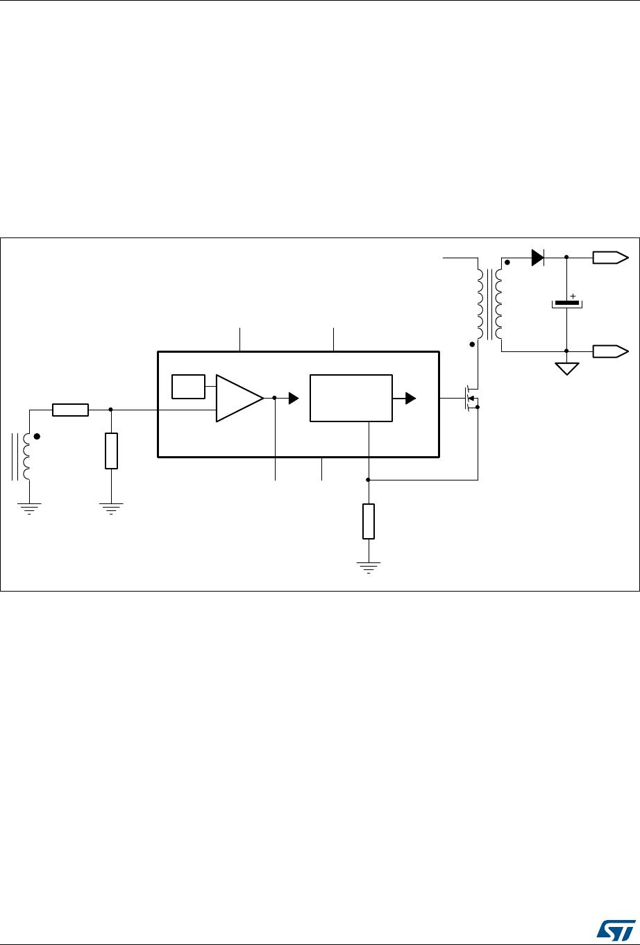
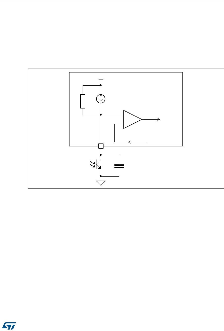
The device is specific for the secondary feedback. The FB pin is connected to an
optocoupler which transmits the error signal from the regulation loop located on the
secondary side of the converter. Typically, a TS431 is used as a voltage reference.
The FB pin is driven directly by the phototransistor's collector to modulate the duty cycle.
The voltage coming from the FB pin is compared with the voltage across the sense resistor,
controlling the peak drain current cycle-by-cycle.
Figure 5. Voltage control principle: internal schematic
6.6 Constant current operation
The voltage of the auxiliary winding is fed into the internal CC block trough the ZCD pin to
achieve an output constant current regulation.
Equation 1 can be used to define the output current in the CC-mode.
Equation 1
This formula shows that the average output current does not depend anymore on the input
or the output voltage, neither on transformer inductance values. The external parameters
defining the output current are the transformer ratio and the sense resistor R
SENSE
. The
current loop gain K
I
is internally defined.
3GC
'SPN3TFOTF
'#
7GC
5P18.-PHJD
$7
*GC
$GC
".
I
OUT
N
PRI
N
SEC
--------------
K
I
2R
SENSE
-----------------------------=
Application information STCH03
14/25 DocID031526 Rev 1
6.7 Voltage feedforward block
The current control structure uses the internal voltage V
C
to define the output current,
according to Equation 1. Actually, the CC comparator will be affected by an internal
propagation delay Td, which will switch off the MOSFET with a peak current higher than the
foreseen value.
The STCH03 device implements a line feedforward function, which solves the issue by
introducing an input voltage dependent offset on the current sense signal, in order to adjust
the cycle-by-cycle current limitation.
The external schematic configuration is shown in Figure 6.
Figure 6. Feedforward compensation: internal schematic
The R
ZCD
resistor can be calculated as follows:
Equation 2
where R
FF
is an internal parameter, defined in Table 5: Electrical characteristics on page 6.
In this case the peak drain current does not depend on input voltage anymore.
3TFOTF
3[DE
7
'#
4&/4&
7%%
$633&/5
$0/530-
(/%
;$%
)7
(%
45$)
"VY
3PWQ
".
R
ZCD
N
AUX
N
PRI
--------------
L
PR
R
FF
T
D
R
SENSE
---------------------------------=
DocID031526 Rev 1 15/25
STCH03 Application information
25
6.8 Burst-mode operation
When the voltage at the FB pin fall to 65 mV below V
FBB
, the burst-mode operation starts:
the MOSFET is turned OFF in order to reduce the consumption. After the MOSFET turns
OFF, the FB pin voltage, as a result of the feedback reaction to the energy delivery stop,
increase up to V
FBB
and the device starts switching again.
During these switching cycles the max peak current is fixed (about V
SENSE_BM
/R
SENSE
) by
an internal clamp inside the current limit circuit. The effect of the burst-mode operation is to
reduce the equivalent switching frequency, which can go down even to few hundred hertz,
minimizing all frequency related losses and making it easier to comply with energy saving
regulations.
This kind of operation, shown in the timing diagrams of Figure 7 along with the other ones, is
audible noise-free since the peak current is low.
Figure 7. Burst-mode operation

STCH03

Mfr. #:
Manufacturer:
STMicroelectronics
Description:
AC/DC Converters Offline PWM controller for low standby adapters
Lifecycle:
New from this manufacturer.
Delivery:
DHL FedEx Ups TNT EMS
Payment:
T/T Paypal Visa MoneyGram Western Union

Products related to this Datasheet