DocID031526 Rev 1 7/25
STCH03 Electrical characteristics
25
V
ZCDT
Triggering voltage Negative-going edge 50 60 70 mV
T
BLANK
Trigger blanking time after MOSFET
turn-on
V
FB
1.65 V 4.3 5.7 7.1
µs
V
FB
= 0.6 V 27.2 32 36.8
T
D-ON
Turn-on delay time after triggering V
GATE
= 6 V, C
GATE
= 1 nF - 270 - ns
T
FORCE
Force turn-on time after blanking - 5.1 6 6.9 µs
LINE FEEDFORWARD
R
FF
Equivalent feedforward resistor I
ZCD
= 1 mA 60 70 80
GATE-DRIVER
V
GDL
Output high voltage
V
DD
= 8.5 V; I
GATE
= 5 mA 7 - -
V
I
GATE
= 5 mA 10.5 13 -
T
RISE
Rising time C
GATE
= 1 nF 70 110 150 ns
T
FALL
Falling time C
GATE
= 1 nF 20 40 60 ns
V
GDL
Output low voltage I
GD-SINK
= 50 mA - - 1 V
FEEDBACK INPUT
V
FBH
Upper saturation - - 3.45 - V
H
FB
Current sense gain - 3.22 3.29 3.36 -
I
FB
Feedback source current - 70 100 130 µA
R
FB
Dynamic feedback resistor - 25 30 41 k
V
FBR
Frequency reduction threshold - 1.4 1.65 1.9 V
V
FBB
Burst-mode threshold
(1)
Voltage falling 0.54 0.6 0.66 V
V
FBF
Exit burst-mode threshold
(1)
0.64 0.72 0.8 V
V
HYST
Burst-mode hysteresis - 50 65 75 mV
CURRENT REFERENCE
V
REFx
Maximum value Internal, not measured - 0.8 - V
K
I
Current loop gain - 0.19 0.2 0.21 V
OVERVOLTAGE PROTECTION
V
OVP
OVP threshold - 2.375 2.5 2.625 V
N
OVP
Consecutive cycles for OVP
triggering
V
OVP
= 2.5 V - 4 - -
UNDERVOLTAGE PROTECTION
V
UVP
UVP threshold - 0.522 0.55 0.578 V
T
UVP
UVP blanking time - 12 20 28 ms
N
UVP
Consecutive cycles for UVP
triggering
V
UVP
= 0.55 V - 4 - -
Table 5. Electrical characteristics (continued)
Symbol Parameter Test condition Min. Typ. Max. Unit
Electrical characteristics STCH03
8/25 DocID031526 Rev 1
CURRENT SENSE
T
LEB
Leading-edge blanking
(1)
V
GATE
= 6 V, C
OUT
= 1 nF 270 380 490 ns
T
D
Gate delay-to-output
(1)
V
GATE
= 6 V, C
OUT
= 1 nF - - 150 ns
V
CSx
Max. clamp value
(1)
dVCS/dt = 200 mV/µs 0.7 0.75 0.8 V
V
OCP
Hiccup-mode OCP level
(1)
0.95 1 1.05 V
V
SENSE_BM
Minimum burst-mode sense voltage - - 72 - mV
FREQUENCY JITTERING
F
D
Modulation frequency - - 9 - kHz
V
ZCDH
Modulation duty cycle - - 50 - %
Ipk Peak current change - - 5 - %
THERMAL SHUTDOWN
T
SD
Thermal shutdown temperature
Guaranteed by design and
characterization
135 150 165 °C
T
HYST
Thermal shutdown hysteresis
Guaranteed by design and
characterization
-30-°C
1. Adjust V
DD
above V
DD-ON
start-up threshold before settings to 14 V.
Table 5. Electrical characteristics (continued)
Symbol Parameter Test condition Min. Typ. Max. Unit
DocID031526 Rev 1 9/25
STCH03 Application information
25
6 Application information
The STCH03 is an off-line CC-mode primary sensing switching controller, specific for offline
quasi-resonant ZVS (zero-voltage-switching at switch turn-on) flyback converters.
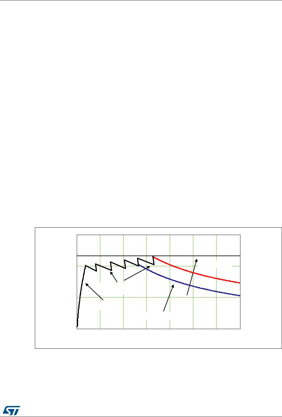
Depending on converter's load condition, the device is able to work in different modes (see
Figure 3):
1. QR mode at heavy load. Quasi resonant operation is achieved by synchronizing the
MOSFET turn-on to the transformer demagnetization by detecting the resulting
negative-going edge of the voltage across any winding of the transformer. Then the
system works close to the boundary between discontinuous (DCM) and continuous
conduction (CCM) of the transformer. As a result, the switching frequency will be
different for different line/load conditions (see the hyperbolic-like portion of the curves
in Figure 3). The minimum turn-on losses, low EMI emission and safe behavior in
short-circuit are the main benefits of this kind of operation.
2. Valley-skipping mode at medium/ light load. Depending on voltage on the FB pin, the
device defines the maximum operating frequency of the converter. As the load is
reduced the MOSFET turn-on will no longer occur on the first valley but on the second
one, the third one and so on. In this way the switching frequency will no longer
increase.
3. Burst-mode with no or very light load. When the load is extremely light or disconnected,
the converter will enter a controlled on/off operation with constant peak current.
Decreasing the load will then result in frequency reduction, which can go down even
reduce to a few hundred hertz, thus minimizing all frequency-related losses and
making it easier to comply with energy saving regulations or recommendations. As the
peak current is very low, no issue of audible noise arises.
Figure 3. Multi-mode operation of STCH03
G
TX
1JONBY
*OQVUWPMUBHF
1
JO
G
PTD
#VSTUNPEF
7BMMFZTLJQQJOH
NPEF
2VBTJSFTPOBOUNPEF
G
TX
1JONBY
*OQVUWPMUBHF
1
JO
G
PTD
#VSTUNPEF
7BMMFZTLJQQJOH
NPEF
2VBTJSFTPOBOUNPEF
G
TX
1JONBY
*OQVUWPMUBHF
1
JO
G
PTD
#VSTUNPEF
7BMMFZTLJQQJOH
NPEF
2VBTJSFTPOBOUNPEF
".

STCH03

Mfr. #:
Manufacturer:
STMicroelectronics
Description:
AC/DC Converters Offline PWM controller for low standby adapters
Lifecycle:
New from this manufacturer.
Delivery:
DHL FedEx Ups TNT EMS
Payment:
T/T Paypal Visa MoneyGram Western Union

Products related to this Datasheet