MAX4845CEYT+

General Description
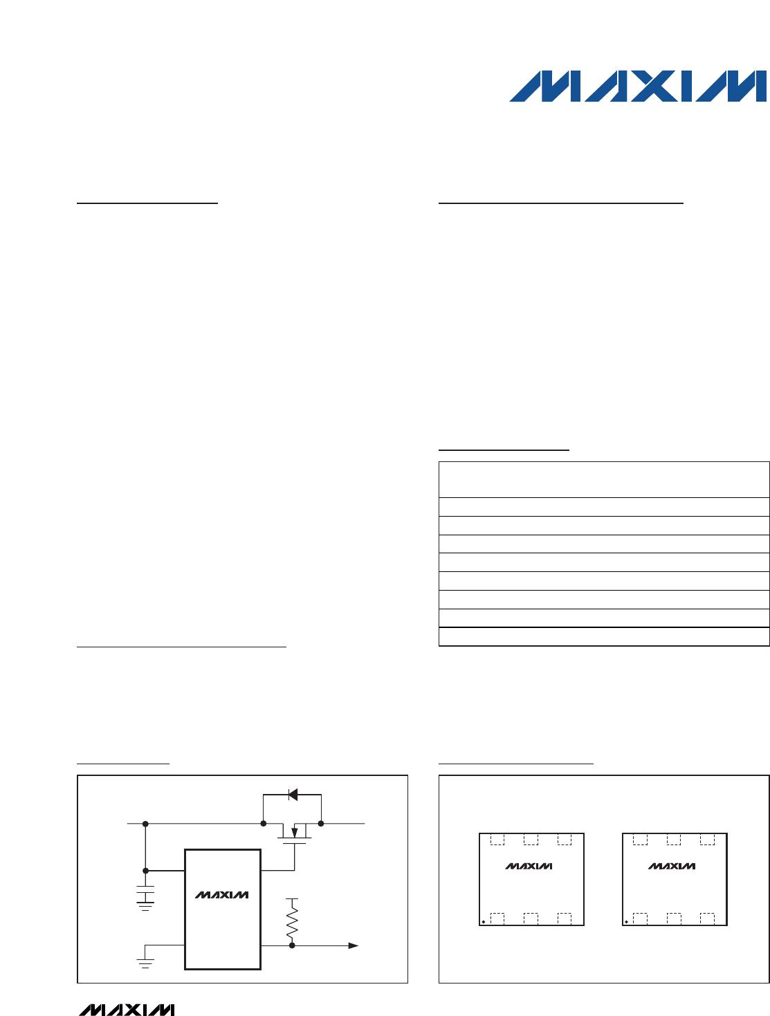
The MAX4843–MAX4846 overvoltage protection con-
trollers protect low-voltage systems against high-voltage
faults of up to 28V. When the input voltage exceeds the
overvoltage threshold, these devices turn off a low-cost,
external n-channel FET(s) to prevent damage to the pro-
tected components. An internal charge pump eliminates
the need for external capacitors and drives the FET gate
for a simple, robust solution.
The overvoltage trip level is set to 7.4V (MAX4843),
6.35V (MAX4844), 5.8V (MAX4845), or 4.65V
(MAX4846). When the input voltage drops below the
undervoltage lockout (UVLO) threshold, the devices
enter a low standby current mode (10µA). The
MAX4843/MAX4844/MAX4845 have a UVLO threshold
of 4.15V, the MAX4845C/MAX4845D have a UVLO
threshold of 2.2V, and the MAX4846 has a UVLO
threshold of 2.5V. In addition to the single FET configu-
ration, the devices can be configured with back-to-
back external FETs to prevent currents from being
back-driven into the adapter.
An additional feature includes a ±15kV ESD-protected
input when bypassed with a 1µF capacitor to ground.
All devices are offered in small 6-pin µDFN (1.5mm x
1.0mm) and 6-pin ultra-thin LGA (MAX4845 and
MAX4846 only) (1.5mm x 1.0mm) packages and are
specified for operation over the -40°C to +85°C temper-
ature range.
Applications
Cell Phones
Digital Still Cameras
PDAs and Palmtop Devices
MP3 Players
Features
Overvoltage Protection Up to 28V
Preset 7.4V, 6.35V, 5.8V, or 4.65V Overvoltage Trip
Level
Low (10µA) Undervoltage Lockout Standby
Current
Drives Low-Cost nMOSFET
Internal 50ms Startup Delay
Internal Charge Pump
Overvoltage Fault FLAG Indicator
6-Pin (1.5mm x 1.0mm) µDFN Package
MAX4843–MAX4846
Overvoltage Protection Controllers with
Low Standby Current
________________________________________________________________
Maxim Integrated Products
1
TOP VIEW
MAX4843–
MAX4846
N.C.
GATE
1
N.C.
GND
FLAG
IN
μDFN
2
3
6
5
4
MAX4845
MAX4846
N.C.
GATE
1
N.C.
GND
FLAG
IN
ULTRA-THIN LGA
2
3
6
5
4
PART
PIN-
PACKAGE
UVLO
(V)
OVLO
(V)
TOP
MARK
MAX4843ELT 6 μDFN 4.15 7.40 BE
MAX4844ELT 6 μDFN 4.15 6.35 BF
MAX4845ELT 6 μDFN 4.15 5.80 BG
MAX4845EYT+T 6 UTLGA 4.15 5.80 AC
MAX4845CEYT+T 6 UTLGA 2.20 5.80 AP
MAX4845DEYT+T 6 UTLGA 2.20 5.80 AQ
MAX4846ELT 6 μDFN 2.50 4.65 BH
MAX4846EYT+T 6 UTLGA 2.50 4.65 AD
Pin Configurations
Ordering Information
MAX4843–
MAX4846
4
OUTPUT
GATE
FLAG
V
IO
N
3
1
IN
2
GND
INPUT
+1.2V TO +28V
1μF
Typical Operating Circuit
19-3649; Rev 5; 12/09
For pricing, delivery, and ordering information, please contact Maxim Direct at 1-888-629-4642,
or visit Maxim’s website at www.maxim-ic.com.
Note: All devices are specified over the -40°C to +85°C tem-
perature range.
+
Denotes a lead(Pb)-free/RoHS-compliant package.
T = Tape and reel.
†OVLO maximum is 6.0V for the MAX4845C and 5.9V for the
MAX4845D.
MAX4843–MAX4846
Overvoltage Protection Controllers with
Low Standby Current
2 _______________________________________________________________________________________
ABSOLUTE MAXIMUM RATINGS
ELECTRICAL CHARACTERISTICS
(V
IN
= +5V for MAX4843/MAX4844/MAX4845, V
IN
= +4V for MAX4846, C
GATE
= 500pF, T
A
= -40°C to +85°C, unless otherwise
noted. Typical values are at T
A
= +25°C.) (Note 1)
Stresses beyond those listed under “Absolute Maximum Ratings” may cause permanent damage to the device. These are stress ratings only, and functional
operation of the device at these or any other conditions beyond those indicated in the operational sections of the specifications is not implied. Exposure to
absolute maximum rating conditions for extended periods may affect device reliability.
IN to GND ..............................................................-0.3V to +30V
GATE to GND ........................................................-0.3V to +12V
FLAG to GND ..........................................................-0.3V to +6V
Continuous Power Dissipation (T
A
= +70°C)
6-Pin µDFN (derate 2.1mW/°C above +70°C) .........167.7mW
6-Pin Ultra-Thin LGA (derate 2.1mW/°C
above +70°C) ...........................................................170.2mW
Operating Temperature Range ..........................-40°C to +85°C
Junction Temperature .................................................... +150°C
Storage Temperature Range ............................-65°C to +150°C
Soldering Temperature (reflow)
6-Pin µDFN...................................................................+240°C
6-Pin Ultra-Thin LGA ....................................................+260°C
PARAMETER SYMBOL CONDITIONS MIN TYP MAX UNITS
Input Voltage Range V
IN
1.2 28.0 V
MAX4843/MAX4844/MAX4845 3.9 4.15 4.4
MAX4845C/MAX4845D 1.8 2.2 2.5
Undervoltage Lockout Threshold UVLO V
IN
falling
MAX4846 2.3 2.5 2.7
V
MAX4843/MAX4844/MAX4845 41
Undervoltage Lockout
Hysteresis
MAX4846 25
mV
MAX4843 7.0 7.4 7.8
MAX4844 6.0 6.35 6.7
MAX4845 5.5 5.8 6.1
MAX4845C 5.5 5.8 6.0
MAX4845D 5.5 5.8 5.9
Overvoltage Trip Level OVLO V
IN
rising
MAX4846 4.35 4.65 4.95
V
MAX4843 75
MAX4844 65
MAX4845 55
Overvoltage Lockout Hysteresis
MAX4846 50
mV
MAX4843/MAX4844/MAX4845 70 120
IN Supply Current I
IN
MAX4846 60 110
μA
V
IN
= 3.8V MAX4843/MAX4844/MAX4845 10 22
UVLO Supply Current I
UVLO
V
IN
= 2.2V MAX4846 8 18
μA
MAX4843/MAX4844/MAX4845 9 9.83 10
Gate Voltage V
GATE
A load
MAX4846 7.5 7.85 8.0
V
GATE Pulldown Current I
PD
V
IN
> OVLO, V
GATE
= 5.5V 10 27 mA
FLAG Output Low Voltage V
OL
I
SINK
= 1mA, FLAG deasserted 0.4 V
FLAG Leakage Current V
FLAG
= 5.5V, FLAG asserted 1 μA
MAX4843–MAX4846
Overvoltage Protection Controllers with
Low Standby Current
_______________________________________________________________________________________ 3
Note 1: All devices are 100% tested at +25°C. Electrical limits across the full temperature range are guaranteed by design and correlation.
ELECTRICAL CHARACTERISTICS (continued)
(V
IN
= +5V for MAX4843/MAX4844/MAX4845, V
IN
= +4V for MAX4846, C
GATE
= 500pF, T
A
= -40°C to +85°C, unless otherwise
noted. Typical values are at T
A
= +25°C.) (Note 1)
PARAMETER SYMBOL CONDITIONS MIN TYP MAX UNITS
TIMING
Startup Delay t
START
V
IN
= UVLO rising to V
GATE
= 0.3V rising
(Figure 1)
20 50 80 ms
FLAG Blanking Time t
BLANK
V
GATE
= 0.3V rising to V
FLAG
= 0.3V falling
(Figure 1)
20 50 80 ms
Gate Turn-On Time t
GON
V
GATE
= 0.3V to 8V
(MAX4843/MAX4844/MAX4845),
V
GATE
= 0.3V to 7V (MAX4846) (Figure 1)
10 ms
Gate Turn-Off Time t
GOFF
V
IN
rising at 1V/μs from 5V to 8V
(MAX4843/MAX4844/MAX4845)
or from 4V to 7V (MAX4846)
to V
GATE
= 0.3V (Figure 2)
6 20 μs
FLAG Assertion Delay t
FLAG
V
IN
rising at 1V/μs from 5V to 8V
(MAX4843/MAX4844/MAX4845)
or from 4V to 7V (MAX4846), to V
FLAG
=
2.4V, R
FLAG
= 10k to 3V (Figure 2)
5.8 μs
Initial Overvoltage Fault Delay t
OVP
V
IN
rising at 1V/μs from 0V to 9V, time from
V
IN
= 5V to I
GATE
= 80% of I
PD
(Figure 3)
1.5 μs
Typical Operating Characteristics
(V
IN
= +5V for MAX4843/MAX4844/MAX4845, V
IN
= +4V for MAX4846, T
A
= +25°C, unless otherwise noted.)
SUPPLY CURRENT vs. SUPPLY VOLTAGE
(MAX4843)
MAX4843-46 toc01
SUPPLY VOLTAGE (V)
SUPPLY CURRENT (μA)
252015105
20
40
60
80
100
0
030
REVERSE CURRENT vs. OUTPUT VOLTAGE
(MAX4843)
MAX4843-46 toc02
OUTPUT VOLTAGE (V)
REVERSE CURRENT (μA)
7
6
4
5
3
2
0.00001
0.0001
0.001
0.01
0.1
1
10
100
1000
0.000001
1
BACK-TO-BACK FET
SINGLE FET
GATE VOLTAGE vs. INPUT VOLTAGE
(MAX4843/MAX4844/MAX4845)
MAX4843-46 toc03
INPUT VOLTAGE (V)
GATE VOLTAGE (V)
7654
3
6
9
12
15
0
38
MAX4843
MAX4844
MAX4845

MAX4845CEYT+

Mfr. #:
Manufacturer:
Maxim Integrated
Description:
Current & Power Monitors & Regulators Overvoltage Protect Controller
Lifecycle:
New from this manufacturer.
Delivery:
DHL FedEx Ups TNT EMS
Payment:
T/T Paypal Visa MoneyGram Western Union