MAX4843–MAX4846
Overvoltage Protection Controllers with
Low Standby Current
6 _______________________________________________________________________________________
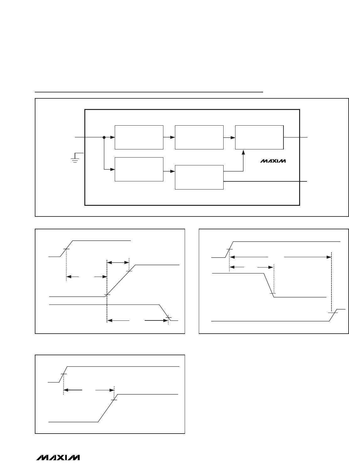
Detailed Description
The MAX4843–MAX4846 provide up to 28V overvoltage
protection for low-voltage systems. When the input volt-
age exceeds the overvoltage trip level, the
MAX4843–MAX4846 turn off a low-cost external n-chan-
nel FET(s) to prevent damage to the protected compo-
nents. An internal charge pump (see the
Functional
Diagram
) drives the FET gate for a simple, robust solu-
tion. On power-up, the device waits for 50ms before dri-
ving GATE high. The open-drain FLAG output is kept at
high impedance for an additional 50ms after GATE goes
high before deasserting. The FLAG output asserts high
immediately to an overvoltage fault.
Undervoltage Lockout (UVLO)
The MAX4843/MAX4844/MAX4845 have a fixed 4.15V
typical UVLO level, the MAX4845C/MAX4845D have a
2.2V typical UVLO, and the MAX4846 has a 2.5V typi-
cal UVLO. When V
IN
is less than the UVLO, the GATE
driver is held low and FLAG is asserted.
Overvoltage Lockout (OVLO)
The MAX4843 has a 7.4V typical OVLO; the MAX4844
has a 6.35V typical OVLO; and the MAX4845 has a
5.8V typical OVLO. The MAX4846 has a 4.65V typical
overvoltage threshold. When V
IN
is greater than OVLO,
the GATE driver is held low and FLAG is asserted.
FLAG Output
The open-drain FLAG output is used to signal to the
host system that there is a fault with the input voltage.
FLAG asserts immediately to an overvoltage fault.
FLAG is held high for 50ms after GATE turns on before
deasserting. Connect a pullup resistor from FLAG to
the logic I/O voltage of the host system.
GATE Driver
An on-chip charge pump is used to drive GATE above
IN, allowing the use of low-cost n-channel MOSFETs. The
charge pump operates from the internal 5.5V regulator.
The actual GATE output voltage tracks approximately
two times V
IN
until V
IN
exceeds 5.5V or the OVLO trip
level is exceeded, whichever comes first. The
MAX4843 has a 7.4V typical OVLO, therefore GATE
remains relatively constant at about 10.5V for 5.5V <
V
IN
< 7.4V. The MAX4845 has a 5.8V typical OVLO, but
this can be as low as 5.5V. The GATE output voltage as
a function of input voltage is shown in the
Typical
Operating Characteristics
.
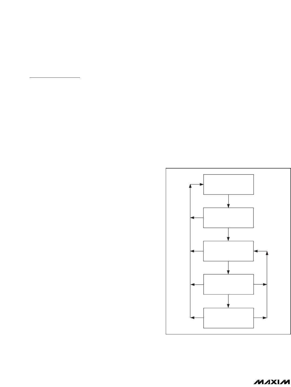
Device Operation
The MAX4843–MAX4846 have an on-board state
machine to control device operation. A flowchart is
shown in Figure 4. On initial power-up, if V
IN
< UVLO or
if V
IN
> OVLO, GATE is held at 0V, and FLAG is high.
If UVLO < V
IN
< OVLO, the device enters startup after
a 50ms internal delay. The internal charge pump is
enabled, and GATE begins to be driven above V
IN
by
the internal charge pump. FLAG is held high during
startup until the FLAG blanking period expires, typically
50ms after the GATE starts going high. At this point the
device is in its on state.
At any time if V
IN
drops below UVLO or V
IN
is greater
than OVLO, FLAG is driven high and GATE is driven
to ground.