MAX7326
I
2
C Port Expander with 12 Push-Pull Outputs
and 4 Inputs
______________________________________________________________________________________ 13
The master can read 2 bytes from the group A ports of the
MAX7326 and then issues a STOP condition (Figure 7). In
this case, the MAX7326 transmits the current port data,
followed by the transition flags. The transition flags are
then cleared, and transition detection restarts. INT goes
high (high impedance if an external pullup resistor is not
fitted) during the slave acknowledge. The new snapshot
data is the current port data transmitted to the master, and
therefore, port transitions occuring during the transmission
are detected. INT remains high until the STOP condition.
A read from the group B ports of the MAX7326 starts
with the master transmitting the group’s slave address
with the R/W bit set high. The MAX7326 acknowledges
the slave address and samples the logic state of the
output ports during the acknowledge bit. The master
can read one or more bytes from the output ports of the
MAX7326, and then issues a STOP condition (Figure 8).
The MAX7326 transmits the current port data, read
back from the actual port outputs (not the port output
latches) during the acknowledge bit. If a port is forced
to a logic state other than its programmed state, the
readback reflects this. If driving a capacitive load, the
readback port level verification algorithms may need to
take the RC rise/fall time into account.
Typically, the master reads one byte from the group B
ports of the MAX7326, then issues a STOP condition
(Figure 8). However, the master can read two or more
bytes from the output ports of the MAX7326, and then
issues a STOP condition. In this case, the MAX7326
resamples the port outputs during each acknowledge
and transmits the new data each time.
SCL
MAX7326 SLAVE ADDRESSSA P1
PORTS
INT OUTPUT
R/W
ACKNOWLEDGE
FROM MAX7326
ACKNOWLEDGE
FROM MASTER
PORT SNAPSHOT
t
IV
t
PH
t
IR
A
O0
O1
I2I3I4I5
O6
O7
D0D1D2D3D4D5D6D7
PORT SNAPSHOT
t
PS
t
IP
F0
F1
F2F3F4F5
F6
F7
D7 D6 D5 D4 D3 D2 D1 D0 A
PORT SNAPSHOT
FLAG
INT REMAINS HIGH UNTIL STOP CONDITION
S = START CONDITION
P = STOP CONDITION
A = ACKNOWLEDGE
Figure 7. Reading Group A Ports of the MAX7326 (2 Data Bytes)
SCL
MAX7326 SLAVE ADDRESS
SA
P
1
ACKNOWLEDGE FROM MAX7326
PORT SNAPSHOT DATA
PORT SNAPSHOT TAKEN
A
P0P1P2P3
DATA 1
P4P5P6P7
D0D1D2D3D4D5D6D7
PORT SNAPSHOT TAKEN
ACKNOWLEDGE
FROM MASTER
R/W
S = START CONDITION
P = STOP CONDITION
A = ACKNOWLEDGE
Figure 8. Reading Group B Ports of the MAX7326
MAX7326
I
2
C Port Expander with 12 Push-Pull Outputs
and 4 Inputs
14 ______________________________________________________________________________________
SCL
SDA
START CONDITION ACKNOWLEDGE
FROM SLAVE
SLAVE ADDRESS
S0
12345678
AAA
t
PV
DATA 1 DATA 2
DATA 2 VALIDDATA 1 VALID
WRITE
TO PORT
DATA OUT
FROM PORT
ACKNOWLEDGE
FROM SLAVE
ACKNOWLEDGE
FROM SLAVE
t
PV
DATA TO PORT DATA TO PORT
R/W
Figure 10. Writing to the Group B Ports of the MAX7326
Writing to the MAX7326
A write to the group A ports of the MAX7326 starts with
the master transmitting the group’s slave address with
the R/W bit set low. The MAX7326 acknowledges the
slave address and samples the ports during the
acknowledge. INT goes high (high impedance if an
external pullup resistor is not fitted) during the slave
address acknowledge. The master can then issue a
STOP condition after the acknowledge (Figure 6), but
typically the master proceeds to transmit one or more
bytes of data. The MAX7326 acknowledges these sub-
sequent bytes of data and updates the four output
ports and the 4-bit interrupt mask register with each
new byte until the master issues a STOP condition
(Figure 9).
A write to the group B ports of the MAX7326 starts with
the master transmitting the group’s slave address with
the R/W bit set low. The MAX7326 acknowledges the
slave address and samples the ports during the
acknowledge bit. The master can now transmit one or
more bytes of data. The MAX7326 acknowledges these
subsequent bytes of data and updates the correspond-
ing group’s ports with each new byte until the master
issues a STOP condition (Figure 10).
SCL
SDA
START CONDITION R/W
SLAVE ADDRESS
S0
12345678
AAA
t
PV
DATA 1 DATA 2
t
PV
DATA TO INTERRUPT MASK DATA TO INTERRUPT MASK
Figure 9. Writing to the Group A Ports of the MAX7326
MAX7326
I
2
C Port Expander with 12 Push-Pull Outputs
and 4 Inputs
______________________________________________________________________________________ 15
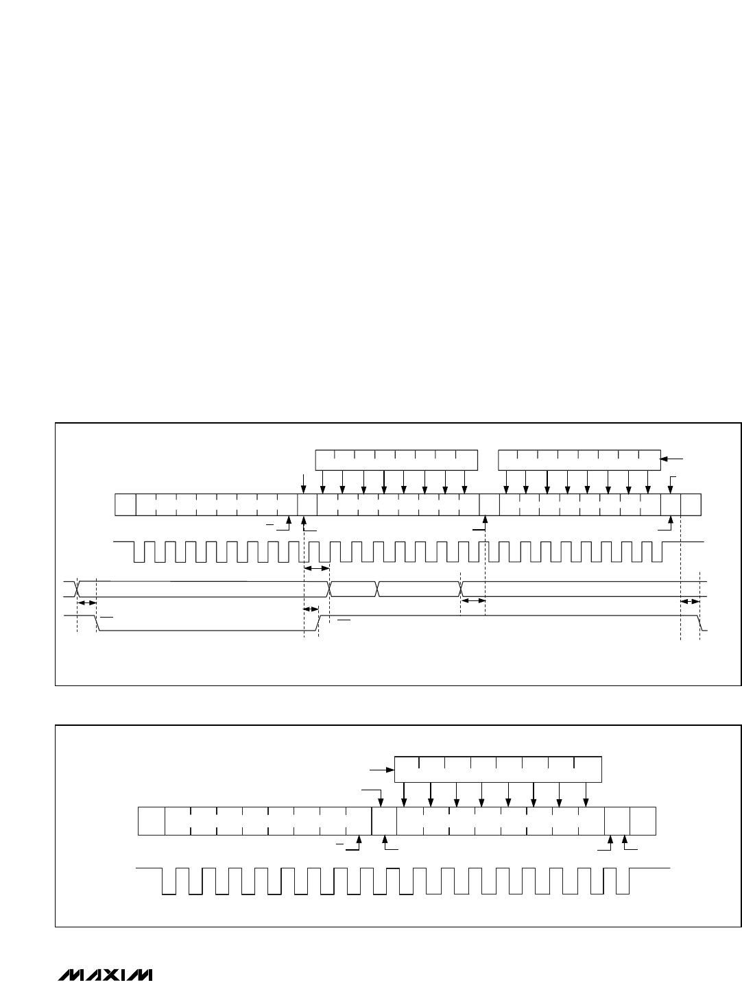
Applications Information
Port Input and I
2
C Interface Level
Translation from Higher or Lower
Logic Voltages
The MAX7326’s SDA, SCL, AD0, AD2, RST, INT, and
I2–I5 are overvoltage protected to +6V independent of
V+. This allows the MAX7326 to operate from a lower
supply voltage, such as +3.3V, while the I
2
C interface
and/or any of the four input ports are driven from a
higher logic level, such as +5V.
The MAX7326 can operate from a higher supply volt-
age, such as +3V, while the I
2
C interface and/or some
of the four input ports I2–I5 are driven from a lower
logic level, such as +2.5V. For V+ < 1.8V, apply a mini-
mum voltage of 0.8 x V+ to assert a logic-high on any
input. For V+ 1.8V, apply a voltage of 0.7 x V+ to
assert a logic-high. For example, a MAX7326 operating
from a +5V supply may not recognize a +3.3V nominal
logic-high. One solution for input level translation is to
drive the MAX7326 inputs from open-drain outputs. Use
a pullup resistor to V+ or a higher supply to ensure a
high logic voltage of greater than 0.7 x V+.
Port Output Signal Level Translation
Each of the push-pull output ports (O0, O1, and
O6–O15) has protection diodes to V+ and GND (Figure
11). When a port output is driven to a voltage higher
than V+ or below GND, the appropriate protection
diode clamps the output to a diode drop above V+ or
below GND. Do not overvolt output ports O0, O1, and
O6–O15. When the MAX7326 is powered down (V+ =
0), each output port appears as a diode clamp to GND
(Figure 11).
Each of the four input ports I2–I5 has a protection diode
to GND (Figure 12). When a port input is driven to a
voltage lower than GND, the protection diode clamps
the output to a diode drop below GND.
Each of the four input ports (I2–I5) also has a 40k
(typ) pullup resistor that can be enabled or disabled.
When a port input is driven to a voltage higher than V+
,
the body diode of the pullup enable switch conducts
and the 40k pullup resistor is enabled. When the
MAX7326 is powered down (V+ = 0), each input port
appears as a 40k resistor in series with a diode con-
nected to zero. Input ports are protected to +6V under
any of these circumstances (Figure 12).
Driving LED Loads
When driving LEDs from one of the 12 output ports (O0,
O1, or O6–O15), a resistor must be fitted in series with
the LED to limit the LED current to no more than 20mA.
Connect the LED cathode to the MAX7326 port, and
the LED anode to V+ through the series current-limiting
resistor, R
LED
. Set the port output low to light the LED.
I2–I5
PULLUP
ENABLE
INPUT
40k
V+
V+
MAX7326
Figure 12. MAX7326 Input Port StructureFigure 11. MAX7326 Push-Pull Output Port Structure
OUTPUT
V+V+
O0, O1,
O6–O15
MAX7326

MAX7326ATG+T

Mfr. #:
Manufacturer:
Maxim Integrated
Description:
Interface - I/O Expanders I2C Port Expander w/12 P-P Out & 4 In
Lifecycle:
New from this manufacturer.
Delivery:
DHL FedEx Ups TNT EMS
Payment:
T/T Paypal Visa MoneyGram Western Union

Products related to this Datasheet