ICS291
TRIPLE PLL FIELD PROG. SPREAD SPECTRUM CLOCK SYNTHESIZER EPROM CLOCK SYNTHESIZER
IDT™ / ICS™
TRIPLE PLL FIELD PROG. SPREAD SPECTRUM CLOCK SYNTHESIZER 3
ICS291 REV F 051310
External Components
The ICS291 requires a minimum number of external
components for proper operation.
Series Termination Resistor
Clock output traces over one inch should use series
termination. To series terminate a 50Ω trace (a commonly
used trace impedance), place a 33Ω resistor in series with
the clock line, as close to the clock output pin as possible.
The nominal impedance of the clock output is 20Ω.
Decoupling Capacitors
As with any high-performance mixed-signal IC, the ICS291
must be isolated from system power supply noise to perform
optimally.
Decoupling capacitors of 0.01µF must be connected
between each VDD and the PCB ground plane. For
optimum device performance, the decoupling capacitor
should be mounted on the component side of the PCB.
Avoid the use of vias on the decoupling circuit.
Crystal Load Capacitors
The device crystal connections should include pads for
small capacitors from X1 to ground and from X2 to ground.
These capacitors are used to adjust the stray capacitance of
the board to match the nominally required crystal load
capacitance. Because load capacitance can only be
increased in this trimming process, it is important to keep
stray capacitance to a minimum by using very short PCB
traces (and no vias) between the crystal and device. Crystal
capacitors must be connected from each of the pins X1 and
X2 to ground.
The value (in pF) of these crystal caps should equal (C
L
-6
pF)*2. In this equation, C
L
= crystal load capacitance in pF.
Example: For a crystal with a 16 pF load capacitance, each
crystal capacitor would be 20 pF [(16-6) x 2 = 20].
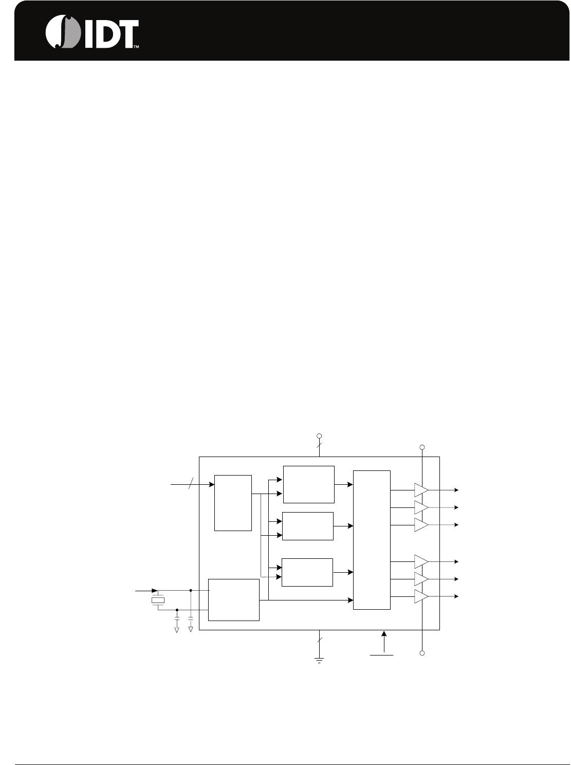
ICS291 Configuration Capabilities
The architecture of the ICS291 allows the user to easily
configure the device to a wide range of output frequencies,
for a given input reference frequency.
The frequency multiplier PLL provides a high degree of
precision. The M/N values (the multiplier/divide values
available to generate the target VCO frequency) can be set
within the range of M = 1 to 1024 and N = 1 to 32,895.
The ICS291 also provides separate output divide values,
from 2 through 63, to allow the two output clock banks to
support widely differing frequency values from the same
PLL.
Each output frequency can be represented as:
Output Drive Control
The ICS291 has two output drive settings. For VDDO=VDD,
low drive should be selected when outputs are less than 100
MHz. High drive should be selected when outputs are
greater than 100 MHz.
For VDDO<2.8 V, high drive should be selected for all output
frequencies.
(Consult the AC Electrical Characteristics for output rise and
fall times for each drive option.)
IDT VersaClock Software
IDT applies years of PLL optimization experience into a user
friendly software that accepts the user’s target reference
clock and output frequencies and generates the lowest jitter,
lowest power configuration, with only a press of a button.
The user does not need to have prior PLL experience or
determine the optimal VCO frequency to support multiple
output frequencies.
VersaClock software quickly evaluates accessible VCO
frequencies with available output divide values and provides
an easy to understand, bar code rating for the target output
frequencies. The user may evaluate output accuracy,
performance trade-off scenarios in seconds.
Spread Spectrum Modulation
The ICS291 utilizes frequency modulation (FM) to distribute
energy over a range of frequencies. By modulating the
output clock frequencies, the device effectively lowers
energy across a broader range of frequencies; thus,
lowering a system’s electromagnetic interference (EMI). The
modulation rate is the time from transitioning from a
minimum frequency to a maximum frequency and then back
to the minimum.
OutputFreq REFFreq
M
N
-----
⋅=