ICS291
TRIPLE PLL FIELD PROG. SPREAD SPECTRUM CLOCK SYNTHESIZER EPROM CLOCK SYNTHESIZER
IDT™ / ICS™
TRIPLE PLL FIELD PROG. SPREAD SPECTRUM CLOCK SYNTHESIZER 4
ICS291 REV F 051310
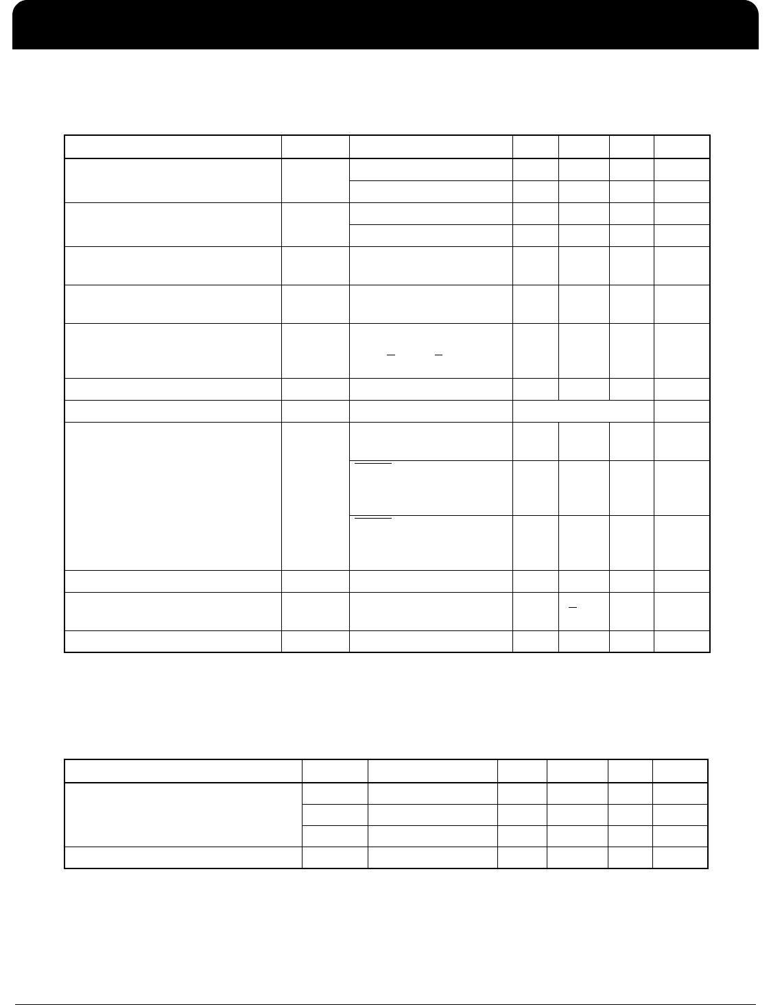
Spread Spectrum Modulation can be applied as either
“center spread” or “down spread”. During center spread
modulation, the deviation from the target frequency is equal
in the positive and negative directions. The effective
average frequency is equal to the target frequency. In
applications where the clock is driving a component with a
maximum frequency rating, down spread should be applied.
In this case, the maximum frequency, including modulation,
is the target frequency. The effective average frequency is
less than the target frequency.
The ICS291 operates in both center spread and down
spread modes. For center spread, the frequency can be
modulated between ±0.125% to ±2.0%. For down spread,
the frequency can be modulated between -0.25% to -4.0%.
Both output frequency banks will utilize identical spread
spectrum percentage deviations and modulation rates, if a
common VCO frequency can be identified.
Spread Spectrum Modulation Rate
The spread spectrum modulation frequency applied to the
output clock frequency may occur at a variety of rates. For
applications requiring the driving of “down-circuit” PLLs,
Zero Delay Buffers, or those adhering to PCI standards, the
spread spectrum modulation rate should be set to 30-33
kHz. For other applications, a 120 kHz modulation option is
available.
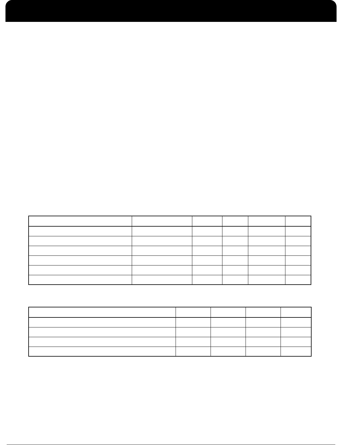
Absolute Maximum Ratings
Stresses above the ratings listed below can cause permanent damage to the ICS291. These ratings, which are
standard values for IDT commercially rated parts, are stress ratings only. Functional operation of the device at these
or any other conditions above those indicated in the operational sections of the specifications is not implied.
Exposure to absolute maximum rating conditions for extended periods can affect product reliability. Electrical
parameters are guaranteed only over the recommended operating temperature range.
Recommended Operation Conditions
Parameter Condition Min. Typ. Max. Units
Supply Voltage, VDD Referenced to GND 7 V
Inputs Referenced to GND -0.5 VDD+0.5 V
Clock Outputs Referenced to GND -0.5 VDD+0.5 V
Storage Temperature -65 150 ° C
Soldering Temperature Max 10 seconds 260 ° C
Junction Temperature 125 ° C
Parameter Min. Typ. Max. Units
Ambient Operating Temperature (ICS291GP) 0 +70 ° C
Ambient Operating Temperature (ICS291GIP) -40 +85 ° C
Power Supply Voltage (measured in respect to GND) +3.135 +3.3 +3.465 V
Power Supply Ramp Time 4 ms
ICS291
TRIPLE PLL FIELD PROG. SPREAD SPECTRUM CLOCK SYNTHESIZER EPROM CLOCK SYNTHESIZER
IDT™ / ICS™
TRIPLE PLL FIELD PROG. SPREAD SPECTRUM CLOCK SYNTHESIZER 5
ICS291 REV F 051310
DC Electrical Characteristics
Unless stated otherwise, VDD = 3.3 V ±5%, Ambient Temperature -40 to +85° C
Note 1: Example with 25 MHz crystal input with six outputs of 33.3
MHz, no load, and VDD = 3.3 V.
Parameter Symbol Conditions Min. Typ. Max. Units
Operating Voltage VDD 3.135 3.465 V
VDDO Voltage VDDO1 and VDDO2 1.80 VDD V
Operating Supply Current IDD
Config. Dependent - See
VersaClock
TM
Estimates
mA
Six 33.3333 MHz outs,
VDD=VDDO=3.3 V;
PDTS
= 1, no load, Note 1
25 mA
PDTS
= 0, no load 500 µA
Input High Voltage V
IH
S2:S0 VDD/2+1 V
Input Low Voltage V
IL
S2:S0 0.4 V
Input High Voltage, PDTS
V
IH
VDD-0.5 V
Input Low Voltage, PDTS
V
IL
0.4 V
Input High Voltage V
IH
ICLK VDD/2+1 V
Input Low Voltage V
IL
ICLK VDD/2-1 V
Output High Voltage
(CMOS High)
V
OH
I
OH
= -4 mA VDD-0.4 V
Output High Voltage V
OH
I
OH
= -8 mA (Low Drive);
I
OH
= -12 mA (High Drive)
2.4
VDDO-0.4
V
Output Low Voltage V
OL
I
OL
= 8 mA (Low Drive);
I
OL
= 12 mA (High Drive)
0.4 V
Short Circuit Current I
OS
Low Drive ±40
mA
High Drive ±70
Nom. Output Impedance Z
O
20
Internal Pull-up Resistor R
PUS
S2:S0, PDTS 190 k
Internal Pull-down
Resistor
R
PD
CLK outputs 120 k
Input Capacitance C
IN
Inputs 4 pF
ICS291
TRIPLE PLL FIELD PROG. SPREAD SPECTRUM CLOCK SYNTHESIZER EPROM CLOCK SYNTHESIZER
IDT™ / ICS™
TRIPLE PLL FIELD PROG. SPREAD SPECTRUM CLOCK SYNTHESIZER 6
ICS291 REV F 051310
AC Electrical Characteristics
Unless stated otherwise, VDD = 3.3 V ±5%, Ambient Temperature -40 to +85° C
Note 1: Measured with 15 pF load.
Note 2: Duty Cycle is configuration dependent. Most configurations are min 45% / max 55%.
Thermal Characteristics
Parameter Symbol Conditions Min. Typ. Max. Units
Input Frequency F
IN
Fundamental crystal 5 27 MHz
Clock input 3 166 MHz
Output Frequency VDDO=VDD 0.314 200 MHz
1.8 V<VDDO<2.8 V 0.314 150 MHz
Output Rise/Fall Time t
OF
80% to 20%, high drive,
Note 1
1.0 ns
Output Rise/Fall Time t
OF
80% to 20%, low drive,
Note 1
2.0 ns
Output Rise/Fall Time t
OF
80% to 20%, high drive,
1.8 V<
VDDO<2.8
Note 2
2.0 ns
Duty Cycle Note 2 40 49-51 60 %
Output Frequency Synthesis Error Configuration Dependent TBD ppm
Power-up time
PLL lock-time from
power-up
410ms
PDTS
goes high until
stable CLK output,
Spread Spectrum Off
0.6 2 ms
PDTS
goes high until
stable CLK output,
Spread Spectrum On
47ms
One Sigma Clock Period Jitter Configuration Dependent 50 ps
Maximum Absolute Jitter t
ja
Deviation from Mean.
Configuration Dependent
+200 ps
Pin-to-Pin Skew Low Skew Outputs -250 250 ps
Parameter Symbol Conditions Min. Typ. Max. Units
Thermal Resistance Junction to
Ambient
θ
JA
Still air 93 ° C/W
θ
JA
1 m/s air flow 78 ° C/W
θ
JA
3 m/s air flow 65 ° C/W
Thermal Resistance Junction to Case θ
JC
20 ° C/W

291PGILFT

Mfr. #:
Manufacturer:
IDT
Description:
Clock Synthesizer / Jitter Cleaner TRIPLE PLL VCXO CLOCK
Lifecycle:
New from this manufacturer.
Delivery:
DHL FedEx Ups TNT EMS
Payment:
T/T Paypal Visa MoneyGram Western Union

Products related to this Datasheet