General Description
The MAX15006/MAX15007 ultra-low quiescent-current
linear regulators are ideal for use in automotive and bat-
tery-operated systems. These devices operate from an
input voltage of 4V to 40V, deliver up to 50mA of output
current, and consume only 10μA of quiescent current at
no load. The internal p-channel pass device keeps the
quiescent current low even at full load. The MAX15007
consumes only 3μA current when in shutdown.
The MAX15006A/MAX15007A have a fixed 3.3V output
while the MAX15006B/MAX15007B have a fixed 5V out-
put voltage. The MAX15006C/MAX15007C feature an
adjustable output from 1.8V to 10V. The MAX15007
includes an enable input to turn the device on or off. All
devices are short-circuit protected and include thermal
shutdown.
The MAX15006/MAX15007 operate over the -40°C to
+125°C automotive temperature range. These devices
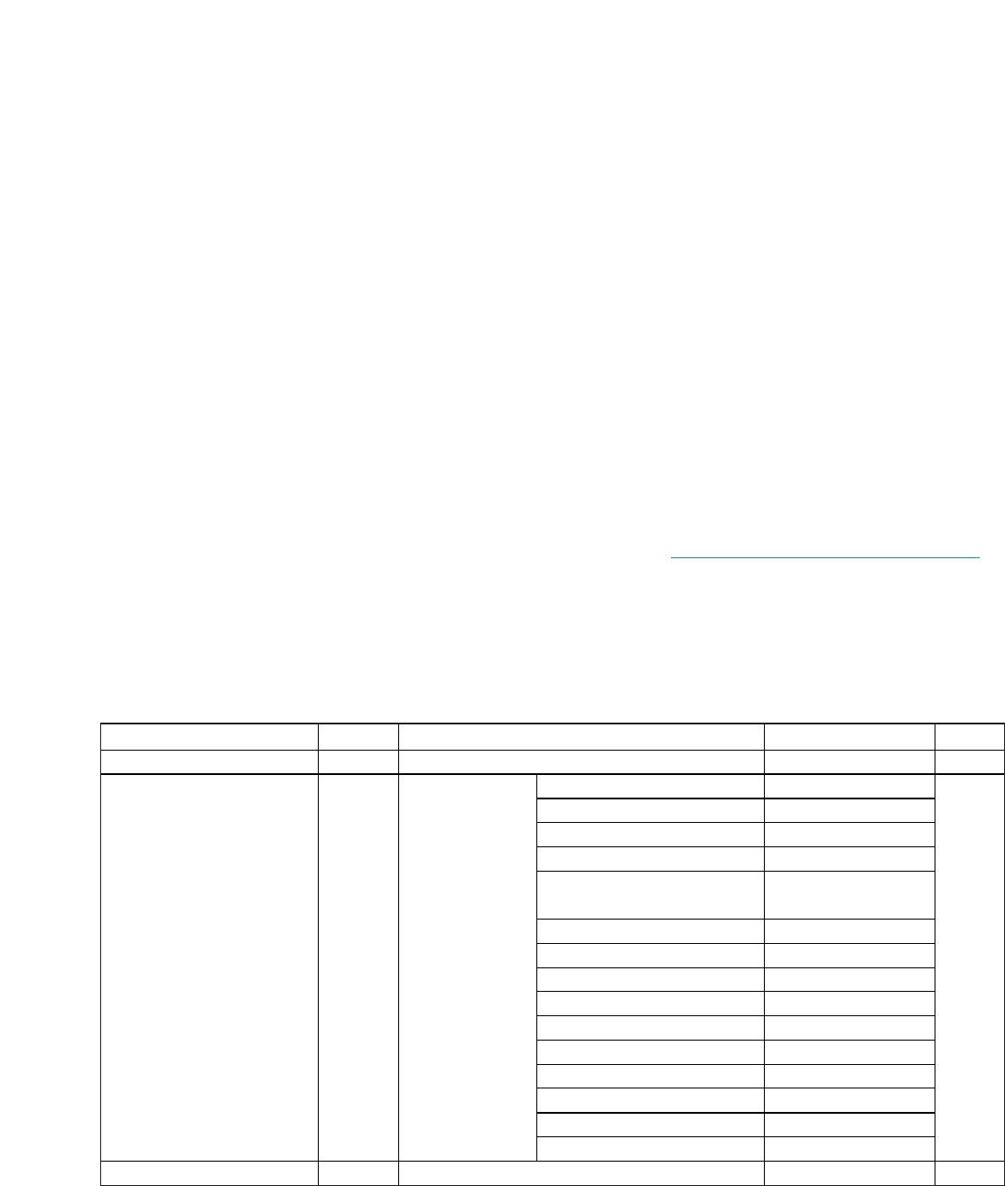
are available in space-saving 3mm x 3mm 6-pin TDFN
and 8-pin SO thermally enhanced packages.
Applications
Automotive
Tire-Pressure Monitoring
Industrial
Telecom
Networking
Features
Wide Operating Input Voltage Range (4V to 40V)
Guaranteed 50mA Output Current
Low Quiescent Current
10µA (No Load) and 90µA (Full Load)
Operates Through Cold-Crank Condition
Withstands 45V Load Dump
Low Dropout Voltage of 300mV
(MAX15006B/MAX15007B)
Stable Operation with Tiny 2.2µF Output Capacitor
Enable Input (MAX15007)
Preset 3.3V and 5.0V Output Voltages
1.8V to 10V Adjustable Output (MAX15006C/
MAX15007C)
Thermal and Short-Circuit Protection
-40°C to +125°C Operating Temperature Range
Thermally Enhanced 3mm x 3mm 6-Pin TDFN/
8-Pin SO Packages
40V, Ultra-Low Quiescent-Current
Linear Regulators in 6-Pin TDFN/8-Pin SO
MAX15006/MAX15007
For pricing, delivery, and ordering information, please contact Maxim Direct at
1-888-629-4642, or visit Maxim Integrated’s website at www.maximintegrated.com.
IN
OUT GND
N.C.IN
OUT (FB)
MAX15006A
MAX15006B
MAX15006C
123
EP
654
TDFN
+
+
TOP VIEW
N.C.
GND
EP
N.C.
1
2
8
7
OUT
N.C. (FB)N.C.
N.C.
IN
( ) FOR MAX15006C ONLY.
SO
3
4
6
5
MAX15006A
MAX15006B
MAX15006C
Pin Configurations
19-0663; Rev 6; 1/13
Pin Configurations continued at end of data sheet.
Ordering Information
Ordering Information continued at end of data sheet.
+
Denotes a lead(Pb)-free/RoHS-compliant package.
/V denotes an automotive qualified part.
*
EP = Exposed pad.
PART TEMP RANGE
PIN-
PACKAGE
TOP
MARK
MAX15006AASA+ -40°C to +125°C 8 SO-EP*
MAX15006AASA/V+ -40°C to +125°C 8 SO-EP*
MAX15006AATT+ -40°C to +125°C 6 TDFN-EP* APE
MAX15006AATT/V+ -40°C to +125°C 6 TDFN-EP* AUR
40V, Ultra-Low Quiescent-Current
Linear Regulators in 6-Pin TDFN/8-Pin SO
2 Maxim Integrated
MAX15006/MAX15007
ABSOLUTE MAXIMUM RATINGS
ELECTRICAL CHARACTERISTICS
(V
IN
= 14V, I
OUT
= 1mA, C
IN
= 0.1µF, C
OUT
= 2.2µF, T
A
= T
J
= -40°C to +125°C, unless otherwise noted. Typical specifications are at
T
A
= +25°C.) (Note 2)
Stresses beyond those listed under “Absolute Maximum Ratings” may cause permanent damage to the device. These are stress ratings only, and functional
operation of the device at these or any other conditions beyond those indicated in the operational sections of the specifications is not implied. Exposure to
absolute maximum rating conditions for extended periods may affect device reliability.
Note 1: Package thermal resistances were obtained using the method described in JEDEC specification JESD51-7, using a four-layer
board. For detailed information on package thermal considerations, refer to www.maximintegrated.com/thermal-tutorial
.
IN to GND ...............................................................-0.3V to +45V
EN to GND..............................................................-0.3V to +45V
OUT, FB to GND.....................................................-0.3V to +12V
OUT Short-Circuit Duration ........................................Continuous
Maximum Current Into Any Pin (except IN and OUT) ......±50mA
Continuous Power Dissipation (T
A
= +70°C)
TDFN (derate 23.8mW/°C above +70°C) ........................1904mW
SO (derate 23.3mW/°C above +70°C)..........................1860mW
Operating Temperature Range .........................-40°C to +125°C
Junction Temperature......................................................+150°C
Storage Temperature Range .............................-65°C to +150°C
Lead Temperature (soldering, 10s) .................................+300°C
Soldering Temperature (reflow) .......................................+260°C
PACKAGE THERMAL CHARACTERISTICS (Note 1)
TDFN
Junction-to-Ambient Thermal Resistance (θ
JA
) ...........42°C/W
Junction-to-Case Thermal Resistance (θ
JC
) ...............8.5°C/W
SO
Junction-to-Ambient Thermal Resistance (θ
JA
) ...........43°C/W
Junction-to-Case Thermal Resistance (θ
JC
) ..................7°C/W
PARAMETER SYMBOL CONDITIONS MIN TYP MAX UNITS
Input Voltage Range V
IN
4 40 V
I
OUT
= 0A (MAX15006A/B/D) 10 17
I
OUT
= 0A (MAX15006C) 8 15
I
OUT
= 0A (MAX15007A/B) 11 18
I
OUT
= 0A (MAX15007C) 9 16
I
OUT
= 100μA
(MAX15006A/B/D)
10.5 18
I
OUT
= 100μA (MAX15006C) 8.5 16
I
OUT
= 100μA (MAX15007A/B) 11.5 19
I
OUT
= 100μA (MAX15007C) 9.5 17
I
OUT
= 1mA (MAX15006A/B/D) 12 20
I
OUT
= 1mA (MAX15006C) 10 18
I
OUT
= 1mA (MAX15007A/B) 13 21
I
OUT
= 1mA (MAX15007C) 11 19
I
OUT
= 50mA (MAX15006) 90 150
I
OUT
= 50mA (MAX15007) 93 150
Ground Current I
GND
Regulator on,
measured at GND
I
OUT
= 60mA (MAX15006D) 110 150
μA
Shutdown Supply Current I
SHDN
Regulator off (MAX15007 only) 3 5 μA
40V, Ultra-Low Quiescent-Current
Linear Regulators in 6-Pin TDFN/8-Pin SO
Maxim Integrated 3
MAX15006/MAX15007
Note 2: Limits at T
A
= -40°C are guaranteed by design.
Note 3: Output voltage regulation is guaranteed for I
OUT
5μA.
Note 4: Dropout voltage is defined as (V
IN
- V
OUT
) when V
OUT
is 2% below the value of V
OUT
when V
IN
= V
OUT
+ 3V.
Note 5: For V
OUT
= 3.3V, the 700mV dropout indicates V
OUT
does not reach 2% below V
OUT
at V
IN
= V
OUT
+ 3V at minimum 4V
input voltage.
Note 6: Enable to regulation time is the time the output takes to reach 95% of its final value with V
IN
= 14V and EN is taken from V
IL
to V
IH
in 5ns.
ELECTRICAL CHARACTERISTICS (continued)
(V
IN
= 14V, I
OUT
= 1mA, C
IN
= 0.1μF, C
OUT
= 2.2μF, T
A
= T
J
= -40°C to +125°C, unless otherwise noted. Typical specifications are at
T
A
= +25°C.) (Note 2)
PARAMETER SYMBOL CONDITIONS MIN TYP MAX UNITS
REGULATOR
V
IN
V
OUT
+ V
DO
50
Guaranteed Output Current I
OUT
V
IN
V
OUT
+ V
DO
(MAX15006D only) 60
mA
MAX15006A/D, MAX15007A 3.25 3.3 3.35
MAX15006B/MAX15007B 4.925 5.0 5.075
Output Voltage (Note 3) V
OUT
I
OUT
= 1mA
MAX15006C/MAX15007C 1.8 10
V
I
OUT
= 5mA, MAX15006B/MAX15007B 30 53
I
OUT
= 5mA, MAX15006C/MAX15007C 30 60
I
OUT
= 50mA, MAX15006B/MAX15007B 300 525
I
OUT
= 50mA, MAX15006C/MAX15007C 300 600
I
OUT
= 50mA, MAX15006A/MAX15007A 1000
Dropout Voltage (Notes 4, 5) V
DO
I
OUT
= 60mA, MAX15006D 1000
mV
Line Regulation 6V V
IN
35V, I
OUT
= 1mA 0.25 %
V
IN
= V
OUT
+ 3V, I
OUT
= 100μA to 50mA 0.7 1.5
Load Regulation
V
IN
= V
OUT
+ 3V, I
OUT
= 100μA to 60mA
(MAX15006D)
0.7 1.5
%
Output Current Limit 80 350 mA
V
OUT
= 3.3V 115
Output Voltage Noise
100Hz to 100kHz, I
OUT
=
50mA, C
OUT
= 2.2μF
V
OUT
= 5V 179
μV
RMS
Power-Supply Rejection Ratio PSRR f = 100Hz, V
IN_RIPPLE
= 500mV
P-P
, I
OUT
= 50mA 66 dB
FB Threshold Voltage V
FB
I
LOAD
= 1mA (MAX15006C/MAX15007C only) 1.2 1.23 1.26 V
FB Input Current I
FB
V
FB
= 0V, 1.5V (MAX15006C/MAX15007C only) -100 +100 nA
ENABLE LOGIC
V
IL
0.4
Enable Threshold Voltage
V
IH
1.4
V
Enable Threshold Hysteresis 60 mV
Enable Pulldown Current Internally pulled down to GND 0.5 μA
Enable to Regulation Time (Note 6) 0.4 2 ms
THERMAL SHUTDOWN
Thermal Shutdown T
SHDN
Junction temperature rising +165 °C
Thermal Shutdown Hysteresis T
HYST
20 °C

MAX15007CATT/V+

Mfr. #:
Manufacturer:
Maxim Integrated
Description:
Linear Voltage Regulators 40V, Ultra-Low Quiescent-Current Linear Regulators in 6-Pin TDFN/8-Pin SO
Lifecycle:
New from this manufacturer.
Delivery:
DHL FedEx Ups TNT EMS
Payment:
T/T Paypal Visa MoneyGram Western Union