40V, Ultra-Low Quiescent-Current
Linear Regulators in 6-Pin TDFN/8-Pin SO
10 Maxim Integrated
MAX15006/MAX15007
Applications Information
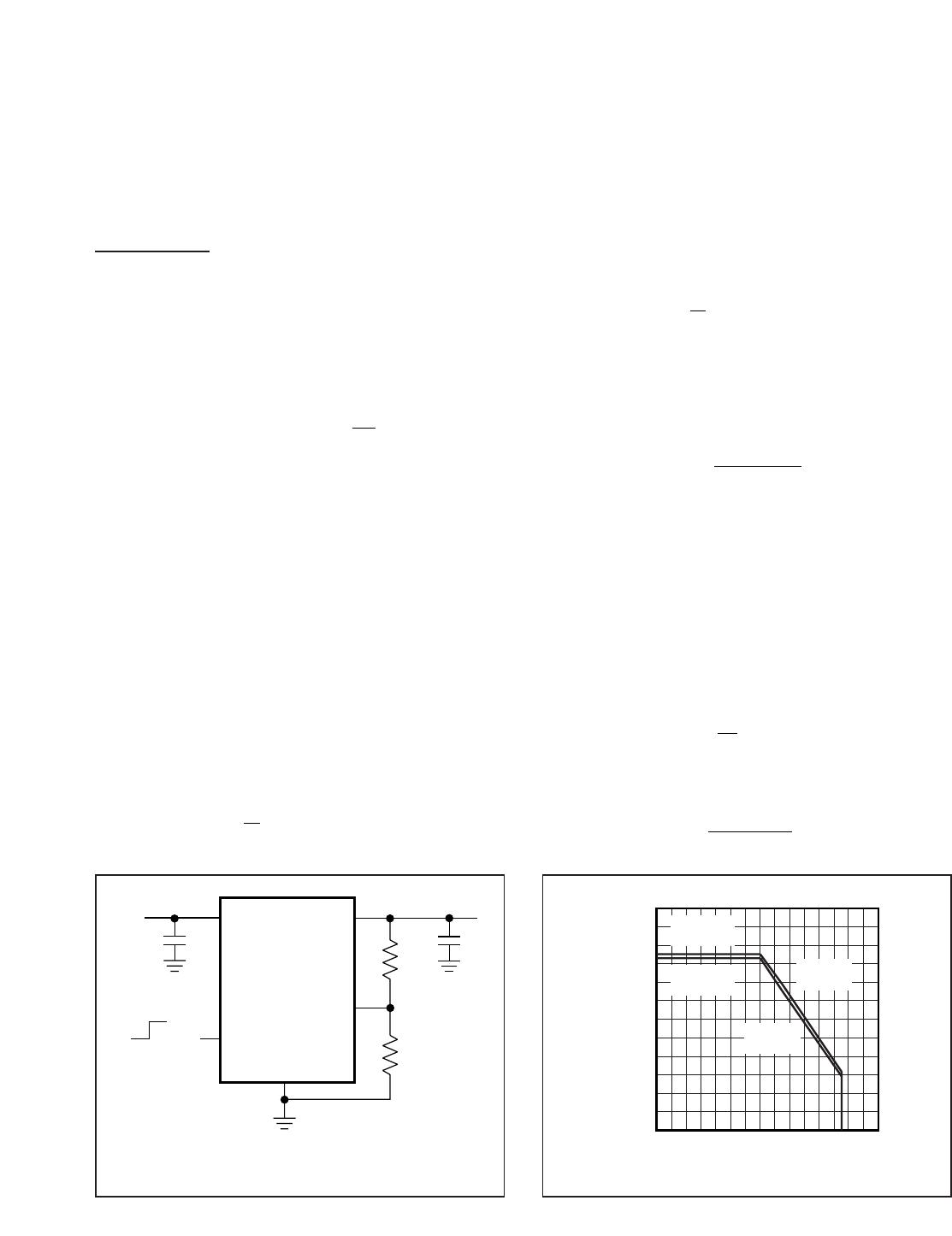
Output Voltage Setting
The MAX15006C/MAX15007C provide an adjustable
output voltage from 1.8V to 10V and do not operate in a
preset output voltage mode. Connect an external resis-
tive divider from OUT to FB to GND as shown in Figure
4 to set the desired output voltage. V
OUT
is calculated
as follows:
where V
FB
= 1.23V and a 5μA minimum current is
required in the external divider for stability.
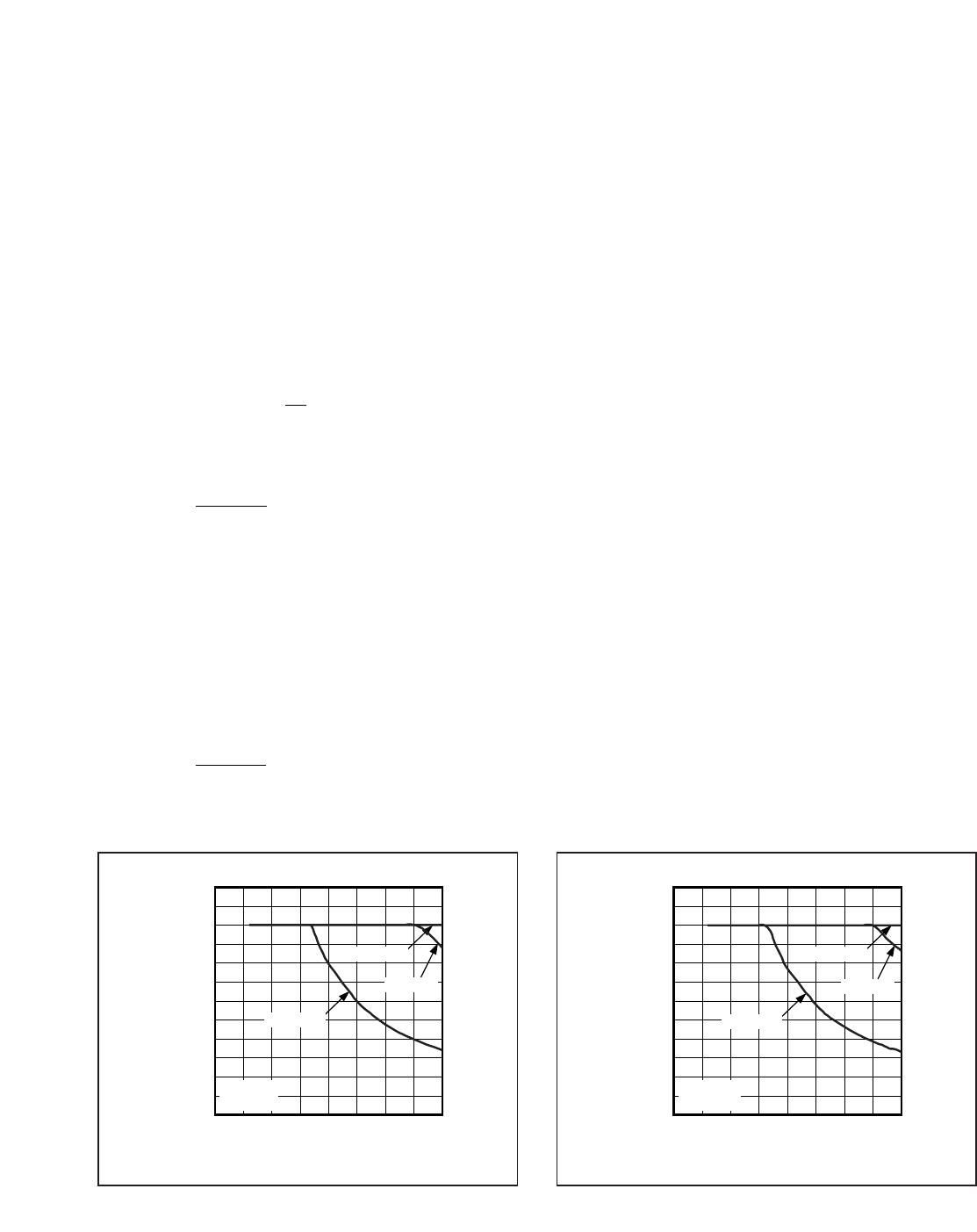
Available Output Current Calculation
The MAX15006/MAX15007 provide up to 50mA of contin-
uous output current. The input voltage range extends to
40V. Package power dissipation limits the amount of out-
put current available for a given input/output voltage and
ambient temperature. Figure 5 shows the maximum
allowable power dissipation for these devices to keep the
junction temperature below +150°C. Figure 5 assumes
that the exposed metal pad of the MAX15006/MAX15007
is soldered to 1in
2
of PCB copper.
Use Figure 5 to determine the allowable package dissi-
pation for a given ambient temperature. Alternately, use
the following formulas to calculate the allowable pack-
age dissipation. For the TDFN package:
For the SO-EP package:
After determining the allowable package dissipation,
calculate the maximum allowable output current, with-
out exceeding the +150°C junction temperature, using
the following formula:
The above equations do not include the negligible
power dissipation from self-heating due to the IC
ground current.
Example 1 (TDFN Package):
T
A
= +125°C
V
IN
= 26V
V
OUT
= 3.3V
Calculate the maximum allowable package dissipation
at the given temperature as follows:
And establish the maximum output current:
I
595.8mW
26V 3.3V
26.2mA
OUT(MAX)
=
=
P 1.9048W 0.0238
W
C
125 C 70 C 5
D
=−
°
°−°
()
= 995.8mW
I
P
VV
50mA
OUT(MAX)
D
IN OUT
=
P
D
.
..
=
≤+ °
1 8605 70
1 8605 0 0233
WforT C
W
A
WW
C
xT Cfor C T C
AA
°
°
()
< + °
70 70 125
P
D
.
..
=
≤+ °
1 9048 70
1 9048 0 0238
WforT C
W
A
WW
C
xT Cfor C T C
AA
°
°
()
< + °
70 70 125
VV1
R1
R2
OUT FB
+
MAX15006 fig04
TEMPERATURE (°C)
P
D
(W)
140
120
100
40
60
80
20
0.2
0.4
0.6
0.8
1.0
1.2
1.4
1.6
1.8
2.0
2.2
2.4
0
0
1.9408W
(6-PIN TDFN)
1.8605W
(8-PIN SO-EP)
DERATE
23.8mW/°C
DERATE
23.3mW/°C
Figure 5. Calculated Maximum Power Dissipation vs. Ambient
Temperature
R1
2.2μF0.1μF
OFF
ON
+1.8V TO +10V
V
OUT
= V
FB
(1 + R1/R2)
V
FB
= 1.23V
+4V TO +40V
R2
IN
EN
GND
OUT
FB
MAX15007C
Figure 4. Setting the Adjustable Output Voltage
40V, Ultra-Low Quiescent-Current
Linear Regulators in 6-Pin TDFN/8-Pin SO
Maxim Integrated 11
MAX15006/MAX15007
Example 2 (TDFN Package):
T
A
= +85°C
V
IN
= 14V
V
OUT
= 5V
Calculate the maximum allowable package dissipation
at the given temperature as follows:
Then determine the maximum output current:
Example 3 (TDFN Package):
T
A
= +50°C
V
IN
= 9V
V
OUT
= 5V
Calculate the maximum allowable package dissipation
at the given temperature as follows:
P
D
= 1.9048W
Find the maximum output current:
In Examples 2 and 3, the maximum output current is
calculated as 172mA and 476mA, respectively; howev-
er, the allowable output current cannot exceed 50mA.
Alternately, use Figures 6a and 6b to quickly determine
the maximum allowable output current for selected
ambient temperatures and input voltages.
Output-Capacitor Selection
and Regulator Stability
For stable operation over the full temperature range
and with load currents up to 50mA, use a low-ESR
2.2μF (min) ceramic or tantalum output capacitor. Use
larger output-capacitor values such as 22μF to reduce
noise, improve load-transient response, and power-
supply rejection.
Some ceramic dielectrics exhibit large capacitance and
ESR variations with temperature. Ensure the minimum
capacitance under worst-case conditions does not
drop below 1.3μF to ensure output stability. With an
X7R dielectric, 2.2μF should be sufficient at all operat-
ing temperatures.
I
1.9048W
9V 5V
476mA
OUT(MAX)
(
=
=⇒I
OUT MAX))
= 50mA
I
1.5478W
14V 5V
172mA
OUT(MAX)
(
=
=⇒I
OUT MAXX
mA
)
= 50
P 1.9048W 0.0238
W
C
85 C 70 C 1.
D
=−
°
°−°
()
= 55478W
MAX15006 fig05a
V
IN
(V)
I
OUT(MAX)
(mA)
353020 2510 155
5
10
15
20
25
30
35
40
45
50
55
60
0
040
T
A
= +85°C
T
A
= +70°C
T
A
= +125°C
V
OUT
= 5V
6-PIN TDFN
Figure 6a. Calculated Maximum Output Current vs. Input
Voltage (6-Pin TDFN-EP)
MAX15006 fig05b
V
IN
(V)
I
OUT(MAX)
(mA)
353020 2510 155
5
10
15
20
25
30
35
40
45
50
55
60
0
040
T
A
= +85°C
T
A
= +70°C
T
A
= +125°C
V
OUT
= 5V
8-PIN SO-EP
Figure 6b. Calculated Maximum Output Current vs. Input
Voltage (8-Pin SO-EP)
40V, Ultra-Low Quiescent-Current
Linear Regulators in 6-Pin TDFN/8-Pin SO
12 Maxim Integrated
MAX15006/MAX15007
TOP VIEW
IN
OUT GND
ENIN
OUT (FB)
MAX15007A
MAX15007B
MAX15007C
123
654
TDFN
+
+
N.C.
GND
EP
EP
N.C.
( ) FOR MAX15007C ONLY.
1
2
8
7
OUT
N.C. (FB)N.C.
EN
IN
SO
3
4
6
5
MAX15007A
MAX15007B
MAX15007C
Pin Configurations (continued)
PART
ENABLE INPUT
FIXED OUTPUT
VOLTAGE (V)
ADJUSTABLE OUTPUT
VOLTAGE (V)
PIN-PACKAGE
MAX15006AASA+ 3.3 8 SO-EP
MAX15006AATT+ 3.3 6 TDFN-EP
MAX15006BASA+ 5 8 SO-EP
MAX15006BATT+ 5 6 TDFN-EP
MAX15006CASA+ ADJ (1.8 to 10) 8 SO-EP
MAX15006CATT+ ADJ (1.8 to 10) 6 TDFN-EP
MAX15007AASA+ 3.3 8 SO-EP
MAX15007AATT+ 3.3 6 TDFN-EP
MAX15007BASA+ 5 8 SO-EP
MAX15007BATT+ 5 6 TDFN-EP
MAX15007CASA+ ADJ (1.8 to 10) 8 SO-EP
MAX15007CATT+ ADJ (1.8 to 10) 6 TDFN-EP
Selector Guide

MAX15007CATT/V+

Mfr. #:
Manufacturer:
Maxim Integrated
Description:
Linear Voltage Regulators 40V, Ultra-Low Quiescent-Current Linear Regulators in 6-Pin TDFN/8-Pin SO
Lifecycle:
New from this manufacturer.
Delivery:
DHL FedEx Ups TNT EMS
Payment:
T/T Paypal Visa MoneyGram Western Union