14
LTC1287
1287fa
U
S
A
O
PP
L
IC
AT
I
WU
U
I FOR ATIO
curve of Noise Error vs Reference Voltage shows the
LSB contribution of this 200µV of noise.
For operation with a 2.5V reference, the 200µV noise is
only 0.32LSB peak-to-peak. Here the LTC1287 noise
will contribute virtually no uncertainty to the output
code. For reduced references, the noise may become a
significant fraction of an LSB and cause undesirable
jitter in the output code. For example, with a 1.25V
reference, this 200µV noise is 0.64LSB peak-to-peak.
This will reduce the range of input voltages over which
a stable output code can be achieved by 0.64LSB. Now
averaging readings may be necessary.
This noise data was taken in a very clean test fixture.
Any setup induced noise (noise or ripple on V
CC
, V
REF
or V
IN
) will add to the internal noise. The lower the
reference voltage used, the more critical it becomes to
have a noise-free setup.
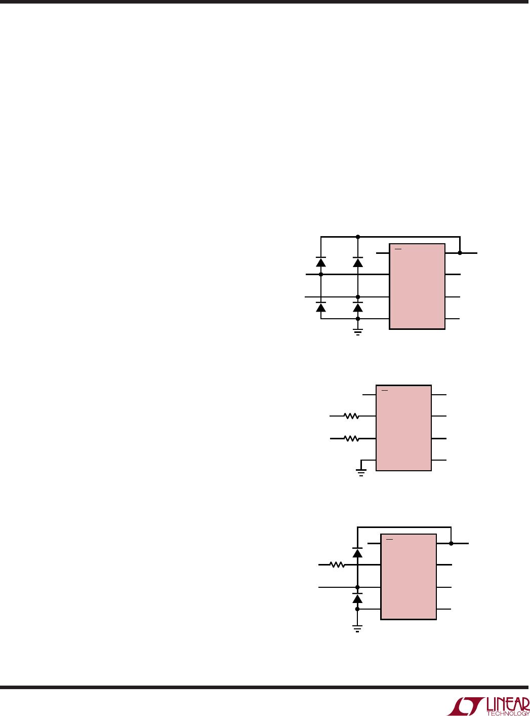
Overvoltage Protection
Applying signals to the LTC1287’s analog inputs that
exceed the positive supply or that go below ground will
degrade the accuracy of the A/D and possibly damage
the device. For example this condition would occur if a
signal is applied to the analog inputs before power is
applied to the LTC1287. Another example is the input
source operating from different supplies of larger value
than the LTC1287. These conditions should be pre-
vented either with proper supply sequencing or by use
of external circuitry to clamp or current limit the input
source. There are two ways to protect the inputs. In
Figure 15 diode clamps from the inputs to V
CC
and GND
are used. The second method is to put resistors in
series with the analog inputs for current limiting. Limit
the current to 15mA per channel. The +IN input can
accept a resistor value of 1k but the –IN input cannot
accept more than 200Ω when clocked at its maximum
clock frequency of 500kHz. If the LTC1287 is clocked at
the maximum clock frequency and 200Ω is not enough
to current limit the input source then the clamp diodes
are recommended (Figures 16 and 17). The reason for
the limit on the resistor value is the MSB bit test is
affected by the value of the resistor placed at the –IN
input (see discussion on Analog Inputs and the Typical
Performance Characteristics curve of Maximum CLK
Frequency vs Source Resistance).
If V
CC
and V
REF
are not tied together, then V
CC
should
be turned on first, then V
REF
. If this sequence cannot be
met, connecting a diode from V
REF
to V
CC
is recom-
mended (see Figure 18).
Because a unique input protection structure is used on
the digital input pins, the signal levels on these pins can
exceed the device V
CC
without damaging the device.
Figure 17. Overvoltage Protection for Inputs
+3V
LTC1287 F17
+IN
GND
V
REF
D
OUT
CLK
V
CC
CS
–IN
LTC1287
1N4148 DIODES
1k
Figure 16. Overvoltage Protection for Inputs
+3V
LTC1287 F16
+IN
GND
V
REF
D
OUT
CLK
V
CC
CS
–IN
200Ω
1k
LTC1287
Figure 15. Overvoltage Protection for Inputs
+3V
LTC1287 F15
+IN
GND
V
REF
D
OUT
CLK
V
CC
CS
–IN
1N4148 DIODES
LTC1287

