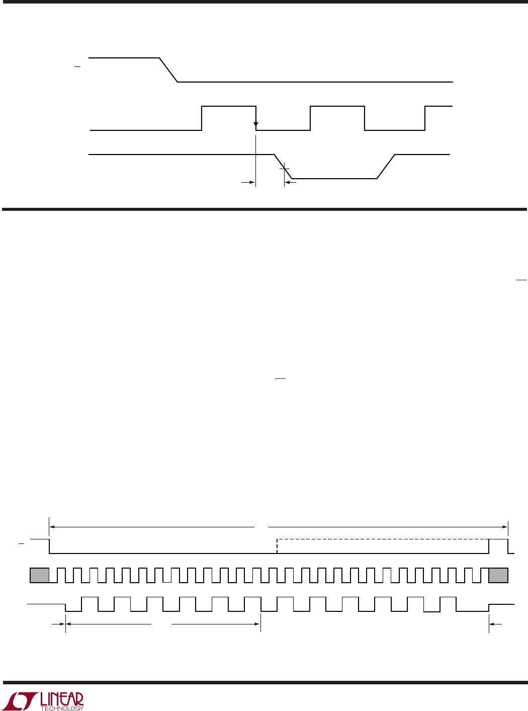
LTC1287
7
1287fa
TEST CIRCUITS
Voltage Waveforms for t
en
U
S
A
O
PP
L
IC
AT
I
WU
U
I FOR ATIO
The LTC1287 is a data acquisition component which
contains the following functional blocks:
1. 12-bit successive approximation capacitive A/D
converter
2. Analog multiplexer (MUX)
3. Sample-and-hold (S/H)
4. Synchronous, half-duplex serial interface
5. Control and timing logic
DIGITAL CONSIDERATIONS
Serial Interface
The LTC1287 communicates with microprocessors and
other external circuitry via a synchronous, half-duplex,
three-wire serial interface (see Operating Sequence). The
clock (CLK) synchronizes the data transfer with each bit
being transmitted on the falling CLK edge. The LTC1287
does not require a configuration input word and has no D
IN
pin. It is permanently configured to have a single differen-
tial input and to operate in unipolar mode. A falling CS
initiates data transfer. The first CLK pulse enables D
OUT
.
After one null bit, the A/D conversion result is output on the
D
OUT
line with a MSB-first sequence followed by a LSB-
first sequence. With the half duplex serial interface the
D
OUT
data is from the current conversion. This provides
easy interface to MSB- or LSB-first serial ports. Bringing
CS high resets the LTC1287 for the next data exchange.
Logic Levels
The logic level standards for this supply range have not
been well defined. What standards that do exist are not
universally accepted. The trip point on the logic inputs of
the LTC1287 is 0.28 × V
CC
. This makes the logic inputs
compatible with HC-type levels and processors that are
D
OUT
0.6V
t
en
B11
CS
CLK
LTC1287 TC07
CLK
t
CYC
CS
B11
B10B9B8
B7
B6
B5B4
B3
B2
B1
B0B1B2
B3
B4
B5B6
B7
B8
B9B10
B11
t
CONV
D
OUT
Hi-Z
t
SMPL
t
SMPL
LTC1287 F01
Figure 1. LTC1287 Operating Sequence
8
LTC1287
1287fa
U
S
A
O
PP
L
IC
AT
I
WU
U
I FOR ATIO
specified at 3.3V. The output D
OUT
is also compatible with
the above standards. The following summarizes such
levels.
V
OH
(no load) V
CC
– 0.1V
V
OL
(no load) 0.1V
V
OH
0.9 × V
CC
V
OL
0.1 × V
CC
V
IH
0.7 × V
CC
V
IL
0.2 × V
CC
The LTC1287 can be driven with 5V logic even when V
CC
is at 3.3V. This is due to a unique input protection device
that is found on the LTC1287.
Microprocessor Interfaces
The LTC1287 can interface directly (without external hard-
ware) to most popular microprocessor (MPU) synchro-
nous serial formats. If an MPU without a serial interface is
used, then three of the MPU’s parallel port lines can be
programmed to form the serial link to the LTC1287. Many
of the popular MPUs can operate with 3V supplies. For
example the MC68HC11 is an MPU with a serial format
(SPI). Likewise parallel MPUs that have the 8051 type
architecture are also capable of operating at this voltage
range. The code for these processors remains the same
and can be found in the LTC1292 data sheet.
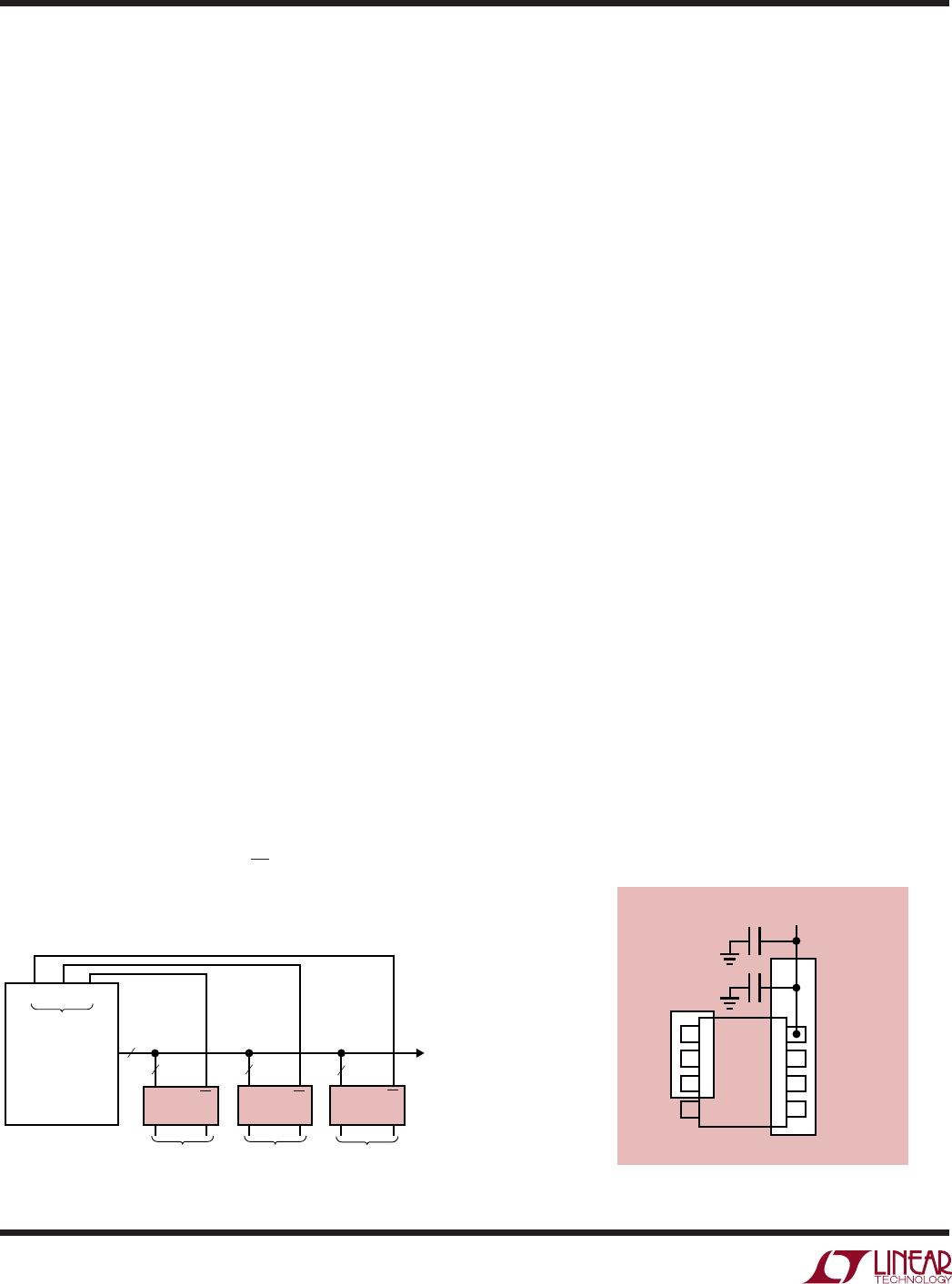
Sharing the Serial Interface
The LTC1287 can share the same two-wire serial interface
with other peripheral components or other LTC1287s
(Figure 2). In this case, the CS signals decide which
LTC1287 is being addressed by the MPU.
Figure 2. Several LTC1287s Sharing One 2-Wire Serial Interface
Figure 3. Example Ground Plane for the LTC1287
LTC1287
2 CHANNELS 2 CHANNELS
2 CHANNELS
CS
CS
CS
2
2
22
2-WIRE SERIAL
INTERFACE TO OTHER
PERIPHERALS OR LTC1287s
2
10
OUTPUT PORT
SERIAL DATA
MPU
LTC1287 F02
LTC1287 LTC1287
1
2
3
4
5
6
7
8
LTC1287
22µF TANTALUM
V
CC
LTC1287 F03
0.1µF
ANALOG CONSIDERATIONS
Grounding
The LTC1287 should be used with an analog ground plane
and single point grounding techniques. Do not use wire
wrapping techniques to breadboard and evaluate the device.
To achieve the optimum performance use a PC board. The
ground pin (Pin 4) should be tied directly to the ground
plane with minimum lead length (a low profile socket is
fine). Pin 7 (V
CC
) should be bypassed to the ground plane
with a 22µF (minimum value) tantalum with leads as short
as possible and as close as possible to the pin. A 0.1µF
ceramic disk also should be placed in parallel with the
22µF and again with leads as short as possible and as close
to V
CC
as possible. Figure 3 shows an example of an ideal
LTC1287 ground plane design for a two-sided board. Of
course this much ground plane will not always be possible,
but users should strive to get as close to this ideal as
possible.
Bypassing
For good performance, V
CC
must be free of noise and
ripple. Any changes in the V
CC
voltage with respect to
ground during a conversion cycle can induce errors or
noise in the output code. V
CC
noise and ripple can be kept
below 0.5mV by bypassing the V
CC
pin directly to the
analog plane with a minimum of 22µF tantalum capacitor
and with leads as short as possible. The lead from the
device to the V
CC
supply also should be kept to a minimum
and the V
CC
supply should have a low output impedance
LTC1287
9
1287fa
U
S
A
O
PP
L
IC
AT
I
WU
U
I FOR ATIO
such as obtained from a voltage regulator (e.g., LT1117).
For high frequency bypassing a 0.1µF ceramic disk placed
in parallel with the 22µF is recommended. Again the leads
should be kept to a minimum. Using a battery to power the
LTC1287 will help reduce the amount of bypass capacitance
required on the V
CC
pin. A battery placed close to the
device will only require 10µF to adequately bypass the
supply pin. Figure 4 shows the effect of poor V
CC
bypassing.
Figure 5 shows the settling of a LT1117 low dropout
regulator with a 22µF bypass capacitor. The noise and
ripple is kept around 0.5mV. Figure 6 shows the response
of a lithium battery with a 10µF bypass capacitor. The
noise and ripple is kept below 0.5mV.
Analog Inputs
Because of the capacitive redistribution A/D conversion
techniques used, the analog inputs of the LTC1287 have
Figure 5. LT1117 Regulator with 22µF Bypassing on V
CC
CS
5V/DIV
V
CC
0.5mV/DIV
HORIZONTAL: 20µs/DIV
Figure 6. Lithium Battery with 10µF Bypassing on V
CC
CS
5V/DIV
V
CC
0.5mV/DIV
HORIZONTAL: 20µs/DIV
capacitive switching input current spikes. These current
spikes settle quickly and do not cause a problem. If large
source resistances are used or if slow settling op amps
drive the inputs, take care to insure the transients caused
by the current spikes settle completely before the
conversion begins.
Source Resistance
The analog inputs of the LTC1287 look like a 100pF
capacitor (C
IN
) in series with a 1.5k resistor (R
ON
). This
value for R
ON
is for V
CC
= 2.7V. With larger supply voltages
R
ON
will be reduced. For example, with V
CC
= 2.7V and V
= –2.7V, R
ON
becomes 500. C
IN
gets switched between
(+) and (–) inputs once during each conversion cycle.
Large external source resistors and capacitances will slow
the settling of the inputs. It is important that the overall RC
time constant is short enough to allow the analog inputs
to settle completely within the allowed time.
Figure 7. Analog Input Equivalent Circuit
HORIZONTAL: 10µs/DIV
Figure 4. Poor V
CC
Bypassing. Noise and
Ripple Can Cause A/D Errors
CS
R
ON
= 1.5k
t
WHCS
+
1/2 CLK
C
IN
=
100pF
LTC1287
“+”
INPUT
R
SOURCE
+
V
IN
+
C1
“–”
INPUT
R
SOURCE
V
IN
C2
LTC1287 F07
VERTICAL: 0.5mV/DIV

LTC1287BCN8#PBF

Mfr. #:
Manufacturer:
Analog Devices Inc.
Description:
Analog to Digital Converters - ADC 3V 12-Bit Single Input, with S/H
Lifecycle:
New from this manufacturer.
Delivery:
DHL FedEx Ups TNT EMS
Payment:
T/T Paypal Visa MoneyGram Western Union

Products related to this Datasheet