General Description
The MAX6854/MAX6855/MAX6856/MAX6858/MAX6860–
MAX6869 ultra-low-current (170nA, typ) microprocessor
(µP) supervisory circuits combine voltage monitoring,
watchdog timer, and manual reset input functions in a 5-
pin SOT23 package. These devices assert a reset signal
whenever the monitored voltage drops below the factory-
trimmed reset threshold voltage, manual reset is assert-
ed, or the watchdog timer expires. The reset output
remains asserted for a minimum timeout period after V
CC
rises above the reset threshold and manual reset is
deasserted. Factory-trimmed reset threshold voltages
are offered from +1.575V to +4.625V in approximately
100mV increments (see the Threshold Suffix Guide).
Each device is offered with six minimum reset timeout
options, ranging from 10ms to 1200ms.
The MAX6854/MAX6855/MAX6856/MAX6858/MAX6860–
MAX6869 are offered in a variety of configurations (see
the Selector Guide). The MAX6854/MAX6855/MAX6856/
MAX6861–MAX6869 provide a manual reset input, MR.
The MAX6864–MAX6869 offer a watchdog timer that
monitors activity at the WDI input to prevent code execu-
tion errors. The MAX6864–MAX6869 offer watchdog
timeout options of 3.3s or 209s (typ). The MAX6861/
MAX6862/MAX6863 feature a pin-selectable reset delay
period of 10ms or 150ms (min). Push-pull active-low,
push-pull active-high, and open-drain active-low reset
outputs are available.
Applications
Portable/Battery-Powered Equipment
PDAs/Cell Phones
MP3 Players/Pagers
Glucose Monitors/Patient Monitors
Features
Ultra-Low 170nA (typ) Supply Current
Reset Thresholds from +1.575V to +4.625V in
Approximately 100mV Increments
Six Minimum Reset Timeout Period Options from
10ms to 1200ms
Manual Reset Option
Watchdog Timer Option
Pin-Selectable 10ms/150ms (min) Reset Timeout
Period (MAX6861/MAX6862/MAX6863)
Immune to Short V
CC
Transients
Guaranteed Reset Valid to V
CC
= +1.1V
Three Reset Output Options:
Push-Pull RESET
Push-Pull RESET
Open-Drain RESET
No External Components
Small 5-Pin SOT23 Package
Pin Compatible to the TPS3836/TPS3837/TPS3838
(MAX6861/MAX6862/MAX6863)
MAX6854/MAX6855/MAX6856/MAX6858/MAX6860–MAX6869
Nanopower µP Supervisory Circuits with
Manual Reset and Watchdog Timer
________________________________________________________________ Maxim Integrated Products 1
Ordering Information
PART
TEMP RANGE
PIN-PACKAGE
MAX6854UK_ _D_-T
-40°C to +85°C
5 SOT23-5
MAX6855UK_ _D_-T
-40°C to +85°C
5 SOT23-5
19-3139; Rev 4; 12/05
For pricing, delivery, and ordering information, please contact Maxim/Dallas Direct! at
1-888-629-4642, or visit Maxim’s website at www.maxim-ic.com.
Ordering Information continued at end of data sheet.
Insert reset threshold suffix (see Table 2, Threshold Suffix
Guide) after UK. Insert the number corresponding to the
desired reset timeout period (see Table 4, Reset Timeout
Period) after D.
Note: Sample stock is generally held on standard versions
only (see Table 5, Standard Versions Table). Standard versions
have an order increment of 2500 pieces. Nonstandard versions
have an order increment of 10,000 pieces. Contact factory for
availability of nonstandard versions.
Devices are available in both leaded and lead-free packaging.
Specify lead-free by replacing “-T” with “+T” when ordering.
Pin Configurations and Selector Guide appear at end of
data sheet.
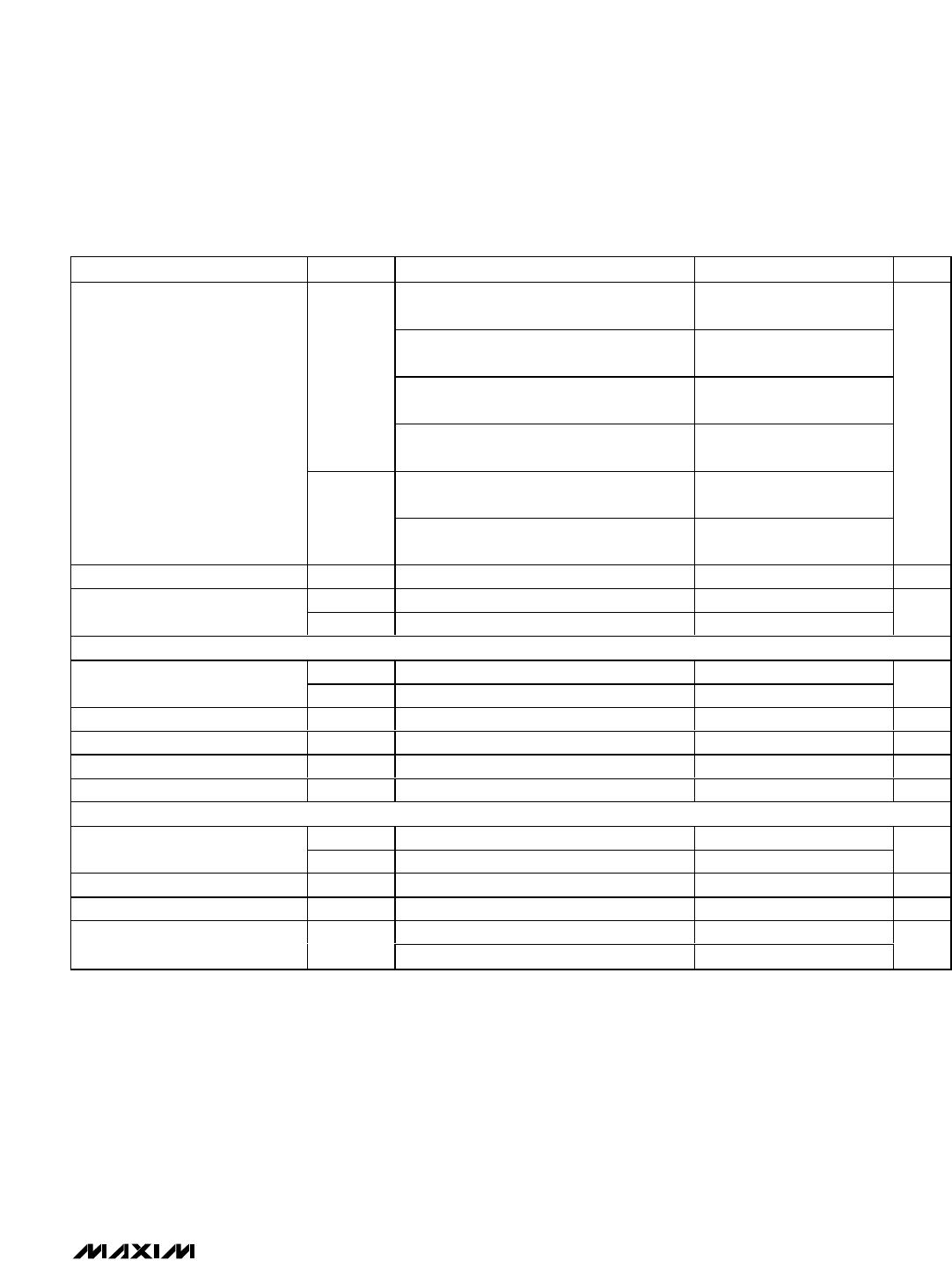
Typical Operating Circuit
MAX6864
MAX6867
µP
V
CC
V
CC
GND
GND
MANUAL
RESET
RESET
I/O
V
CC
0.1µF
RESET
MR
WDI
MAX6854/MAX6855/MAX6856/MAX6858/MAX6860–MAX6869
Nanopower µP Supervisory Circuits with
Manual Reset and Watchdog Timer
2 _______________________________________________________________________________________
ABSOLUTE MAXIMUM RATINGS
ELECTRICAL CHARACTERISTICS
(V
CC
= 1.2V to 5.5V, T
A
= -40°C to +85°C, unless otherwise specified. Typical values are at V
CC
= 2.5V, T
A
= +25°C.) (Note 1)
Stresses beyond those listed under “Absolute Maximum Ratings” may cause permanent damage to the device. These are stress ratings only, and functional
operation of the device at these or any other conditions beyond those indicated in the operational sections of the specifications is not implied. Exposure to
absolute maximum rating conditions for extended periods may affect device reliability.
V
CC
, Open-Drain RESET to GND ..........................-0.3V to +6.0V
MR, Push-Pull RESET, RESET,
WDI, CT, I.C............................................-0.3V to (V
CC
+ 0.3V)
Input Current, Output Current (all pins)............................±20mA
Continuous Power Dissipation (T
A
= +70°C)
5-Pin SOT23 (derate 7.1mW/°C above +70°C)............571mW
Operating Temperature Range ...........................-40°C to +85°C
Junction Temperature .....................................................+150°C
Storage Temperature Range .............................-65°C to +150°C
Lead Temperature (soldering, 10s) .................................+300°C
PARAMETER
SYMBOL
CONDITIONS MIN
TYP
MAX
T
A
0°C 1.1 5.5
Supply Voltage V
CC
T
A
= -40°C to +85°C 1.2 5.5
V
V
CC
= 5.0V 210 400
V
CC
= 3.3V 190 380
V
CC
> V
TH
, no load,
reset output
deasserted (Note 2)
V
CC
= 1.8V 170 370
nA
Supply Current I
CC
V
CC
< V
TH
, no load, reset output asserted
715µA
V
CC
Reset Threshold V
TH
V
CC
falling (see Table 2)
V
TH
-
2.5%
V
TH
V
TH
+
2.5%
V
Reset Threshold Hysteresis V
HYST
Reset asserted to reset deasserted 0.5
D1 10 15 25
D2 40 60 80
D3 150 225 300
D4
1200 1800 2400
D5 300 450 600
Reset Timeout Period t
RP
V
CC
= V
TH
+ 150mV
(Figures 2 and 3)
D6 600 900
1200
ms
V
CC
to Reset Delay t
RD
V
CC
falling from (V
TH
+ 100mV) to
(V
TH
- 100mV) at 10mV/µs
40 µs
V
CC
1.1V, I
SINK
= 50µA,
RESET asserted, T
A
0°C
0.3
V
CC
1.2V, I
SINK
= 100µA,
RESET asserted
0.3
V
OL
V
CC
2.12V, I
SINK
= 1.2mA,
RESET asserted
0.3
V
CC
1.71V, I
SOURCE
= 200µA,
RESET deasserted, push-pull RESET only
0.8 x V
CC
RESET Output Voltage
V
OH
V
CC
2.38V, I
SOURCE
= 500µA,
RESET deasserted, push-pull RESET only
0.8 x V
CC
V
Open-Drain RESET Leakage
Current
I
LKG
RESET deasserted 25 nA
MAX6854/MAX6855/MAX6856/MAX6858/MAX6860–MAX6869
Nanopower µP Supervisory Circuits with
Manual Reset and Watchdog Timer
_______________________________________________________________________________________ 3
ELECTRICAL CHARACTERISTICS (continued)
(V
CC
= 1.2V to 5.5V, T
A
= -40°C to +85°C, unless otherwise specified. Typical values are at V
CC
= 2.5V, T
A
= +25°C.) (Note 1)
PARAMETER
SYMBOL
CONDITIONS MIN
TYP MAX
V
CC
1.1V, I
SOURCE
= 10µA,
RESET asserted, T
A
0°C
0.8 x V
CC
V
CC
1.2V, I
SOURCE
= 10µA,
RESET asserted
0.8 x V
CC
V
CC
1.53V, I
SOURCE
= 200µA,
RESET asserted
0.8 x V
CC
V
OH
V
CC
2.12V, I
SOURCE
= 500µA,
RESET asserted
0.8 x V
CC
V
CC
1.71V, I
SINK
= 500µA,
RESET deasserted
0.3
RESET Output Voltage
V
OL
V
CC
2.38V, I
SINK
= 1.2mA,
RESET deasserted
0.3
V
CT Input Current CT = GND or V
CC
20 nA
V
IH
0.8 x V
CC
CT Input Voltage
V
IL
0.2 x V
CC
V
MANUAL RESET INPUT
V
IH
0.7 x V
CC
MR Input Voltage
V
IL
0.3 x V
CC
V
MR Minimum Pulse Width t
MPW
s
MR Glitch Rejection 200 ns
MR to Reset Delay t
MRD
250 ns
MR Pullup Resistance 51020k
WATCHDOG TIMER (MAX6864–MAX6869)
V
IH
0.7 x V
CC
WDI Input Voltage
V
IL
0.3 x V
CC
V
WDI Input Current WDI = GND or V
CC
20 nA
WDI Pulse Width t
WDI
(Note 3) 150 ns
S 1.5 3.3
7.75
Watchdog Timeout Period t
WD
L95209 487
s
Note 1: Devices are tested at T
A
= +25°C. Specifications for T
A
= -40°C to +85°C are guaranteed by design.
Note 2: For the MAX6864–MAX6869, the watchdog period is 1s with t
RISE
and t
FALL
< 50ns.
Note 3: Guaranteed by design.

MAX6864UK23D3S+T

Mfr. #:
Manufacturer:
Maxim Integrated
Description:
Supervisory Circuits Single nPower Supervisor
Lifecycle:
New from this manufacturer.
Delivery:
DHL FedEx Ups TNT EMS
Payment:
T/T Paypal Visa MoneyGram Western Union