49FCT3805EPYGI

1
IDT49FCT3805D/E
3.3V CMOS DUAL 1-TO-5 CLOCK DRIVER
INDUSTRIAL TEMPERATURE RANGE
MAY 2010
2004 Integrated Device Technology, Inc. DSC-5864/19c
IDT49FCT3805D/E
INDUSTRIAL TEMPERATURE RANGE
3.3V CMOS DUAL
1-TO-5 CLOCK DRIVER
FUNCTIONAL BLOCK DIAGRAM
5
OA
1 - OA5
OB1 - OB5
OEA
INA
OEB
INB
MON
5
PIN CONFIGURATION
OA1
OA3
OA4
GNDQ
INA
VCCA
OA2
GNDA
OA5
OEA
1
2
3
4
5
6
7
8
9
OB3
OB4
MON
IN
B
VCCB
OB1
OB2
GNDB
OB5
OEB
11
12
13
14
15
16
17
18
19
20
10
SSOP/ QSOP
TOP VIEW
FEATURES:
Advanced CMOS Technology
Guaranteed low skew < 200ps (max.)
Very low propagation delay < 2.5ns (max)
Very low duty cycle distortion < 270ps (max)
Very low CMOS power levels
Operating frequency up to 166MHz
TTL compatible inputs and outputs
Inputs can be driven from 3.3V or 5V components
Two independent output banks with 3-state control
1:5 fanout per bank
"Heartbeat" monitor output
•V
CC = 3.3V ± 0.3V
Available in SSOP and QSOP packages
The IDT logo is a registered trademark of Integrated Device Technology, Inc.
DESCRIPTION:
The FCT3805 is a 3.3 volt clock driver built using advanced CMOS
technology. The device consists of two banks of drivers, each with a 1:5 fanout
and its own output enable control. The device has a "heartbeat" monitor for
diagnostics and PLL driving. The MON output is identical to all other outputs
and complies with the output specifications in this document. The FCT3805 offers
low capacitance inputs.
The FCT3805 is designed for high speed clock distribution where signal
quality and skew are critical. The FCT3805 also allows single point-to-point
transmission line driving in applications such as address distribution, where one
signal must be distributed to multiple recievers with low skew and high signal
quality.
For more information on using the FCT3805 with two different input
frequencies on bank A and B, please see AN-236.
2
INDUSTRIAL TEMPERATURE RANGE
IDT49FCT3805D/E
3.3V CMOS DUAL 1-TO-5 CLOCK DRIVER
CAPACITANCE (TA = +25
O
C, f = 1.0MHz)
Symbol Parameter
(1)
Conditions Typ. Max. Unit
CIN Input Capacitance VIN = 0V 3 4 pF
COUT Output Capacitance VOUT = 0V 6 pF
NOTE:
1. This parameter is measured at characterization but not tested.
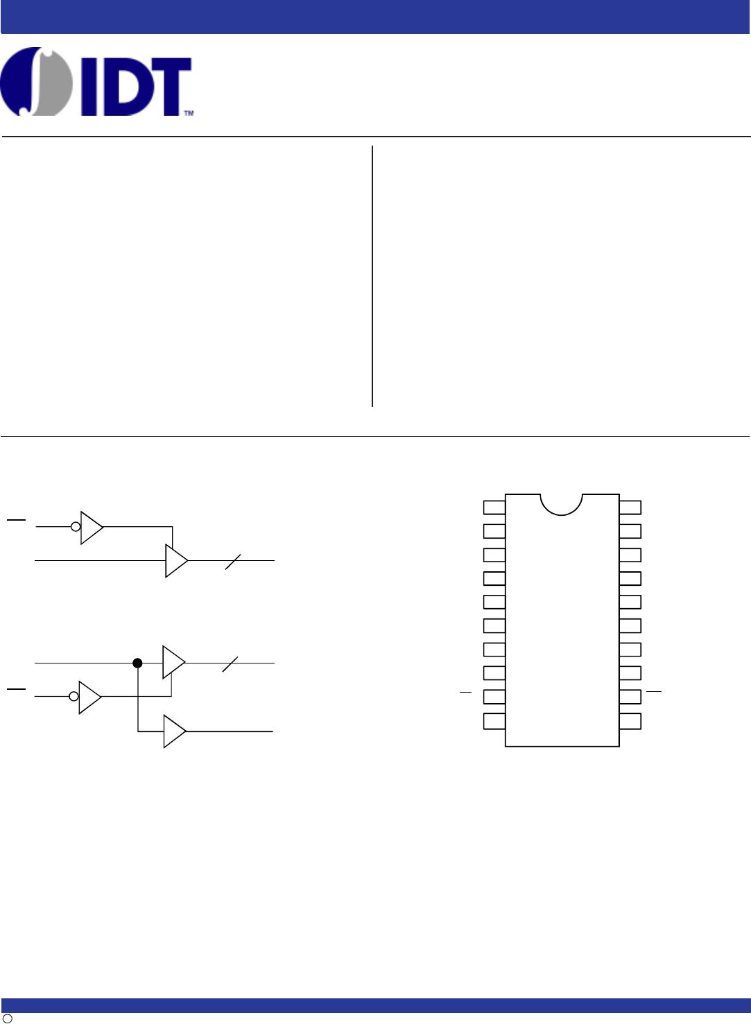
PIN DESCRIPTION
Pin Names Description
OEA, OEB 3-State Output Enable Inputs (Active LOW)
INA, INB Clock Inputs
OAn, OBn Clock Outputs
M O N Monitor Output
FUNCTION TABLE
(1)
Inputs Outputs
OEA, OEB INA, INB OAn, OBn MON
LLLL
LHHH
HLZL
HHZH
NOTE:
1. H = HIGH
L = LOW
Z = High-Impedance
ABSOLUTE MAXIMUM RATINGS
(1)
Symbol Description Max Unit
VCC Input Power Supply Voltage –0.5 to +4.6 V
VI Input Voltage –0.5 to +5.5 V
VO Output Voltage –0.5 to VCC+0.5 V
TJ Junction Temperature 150 ° C
T
STG Storage Temperature –65 to +165 ° C
NOTE:
1. Stresses greater than those listed under ABSOLUTE MAXIMUM RATINGS may cause
permanent damage to the device. This is a stress rating only and functional operation
of the device at these or any other conditions above those indicated in the operational
sections of this specification is not implied. Exposure to absolute maximum rating
conditions for extended periods may affect reliability.
DC ELECTRICAL CHARACTERISTICS OVER OPERATING RANGE
Following Conditions Apply Unless Otherwise Specified
Industrial: TA = -40°C to +85°C, VCC = 3.3V ± 0.3V
Symbol Parameter Test Conditions
(1)
Min. Typ.
(2)
Max. Unit
VIH Input HIGH Level 2 5.5 V
VIL Input LOW Level –0.5 0.8 V
IIH Input HIGH Current VCC = Max. VI = 5.5V ±1
IIL Input LOW Current VCC = Max. VI = GND ±A
IOZH High Impedance Output Current VCC = Max. VO = VCC ——±1
IOZL (3-State Outputs Pins) VO = GND ±1
VIK Clamp Diode Voltage VCC = Min., IIN = –18mA –0.7 –1.2 V
IODH Output HIGH Current VCC = 3.3V, VIN = VIH or VIL, VO = 1.5V
(3,4)
–45 –74 –180 mA
IODL Output LOW Current VCC = 3.3V, VIN = VIH or VIL, VO = 1.5V
(3,4)
50 90 200 mA
IOS Short Circuit Current VCC = Max., VO = GND
(3,4)
–60 –135 –240 mA
VOH Output HIGH Voltage VCC = Min. IOH = –12mA 2.4
(5)
3—
VIN = VIH or VIL IOH = –8mA 2.4
(5)
3—V
IOH = –100µAVCC - 0.2
VOL Output LOW Voltage VCC = Min. IOL = 12mA 0.3 0.4
VIN = VIH or VIL IOL = 8mA 0.2 0.4 V
IOL = 100µA 0.2
NOTES:
1. For conditions shown as Max. or Min., use appropriate value specified under Electrical Characteristics for the applicable device type.
2. Typical values are at VCC = 3.3V, 25°C ambient.
3. Not more than one output should be shorted at one time. Duration of the test should not exceed one second.
4. This parameter is guaranteed but not tested.
5. VOH = Vcc -0.6V at rated current.
3
IDT49FCT3805D/E
3.3V CMOS DUAL 1-TO-5 CLOCK DRIVER
INDUSTRIAL TEMPERATURE RANGE
NOTES:
1. For conditions shown as Max. or Min., use appropriate value specified under Electrical Characteristics for the applicable device type.
2. Typical values are at VCC = 3.3V, +25°C ambient.
3. This parameter is not directly testable, but is derived for use in Total Power Supply calculations.
4. IC = IQUIESCENT + IINPUTS + IDYNAMIC
IC = ICC + ICC DHNT + ICCD (fONO)
ICC = Quiescent Current (ICCL, ICCH and ICCZ)
ICC = Power Supply Current for a TTL High Input (VIN = VCC -0.6V)
DH = Duty Cycle for TTL Inputs High
NT = Number of TTL Inputs at DH
ICCD = Dynamic Current Caused by an Input Transition Pair (HLH or LHL)
fO = Output Frequency
NO = Number of Outputs at fO
POWER SUPPLY CHARACTERISTICS
Symbol Parameter Test Conditions
(1)
Min. Typ.
(2)
Max. Unit
I
CCL Quiescent Power Supply Current VCC = Max. 0.1 30 µA
I
CCH VIN = GND or VCC
ICCZ
ICC Power Supply Current per Input HIGH VCC = Max. 45 300 µA
VIN = VCC –0.6V
I
CCD Dynamic Power Supply Current VCC = Max. VIN = VCC 80 120 µA/MHz
per Output
(3)
CL = 15pF VIN = GND
All Outputs Toggling
IC Total Power Supply Current
(4)
VCC = Max. VIN = VCC 125 150
C
L = 15pF VIN = GND
All Outputs Toggling V
IN = VCC –0.6V 125 150
fi = 133MHz V
IN = GND mA
V
CC = Max. VIN = VCC 155 195
CL = 15pF VIN = GND
All Outputs Toggling VIN = VCC –0.6V 160 195
fi = 166MHz VIN = GND

49FCT3805EPYGI

Mfr. #:
Manufacturer:
IDT
Description:
Clock Drivers & Distribution 3.3V Dual 1:5 Clock Driver
Lifecycle:
New from this manufacturer.
Delivery:
DHL FedEx Ups TNT EMS
Payment:
T/T Paypal Visa MoneyGram Western Union