4
INDUSTRIAL TEMPERATURE RANGE
IDT49FCT3805D/E
3.3V CMOS DUAL 1-TO-5 CLOCK DRIVER
SWITCHING CHARACTERISTICS OVER OPERATING RANGE - 3805D
(3,4)
Symbol Parameter Conditions
(1)
Min.
(2)
Max. Unit
t
PLH Propagation Delay CL = 15pF 1 3 ns
tPHL INA to OAn, INB to OBn f ≤ 133MHz
tR Output Rise Time (0.8V to 2V) — 1.5 ns
tF Output Fall Time (2V to 0.8V) — 1.5 ns
tSK(O) Same device output pin to pin skew
(5)
— 270 ps
tSK(P) Pulse skew
(6,9)
— 270 ps
tSK(PP) Part to part skew
(7)
— 550 ps
t
PZL Output Enable Time — 5.2 ns
tPZH OEA to OAn, OEB to OBn
tPLZ Output Disable Time — 5.2 ns
tPHZ OEA to OAn, OEB to OBn
fMAX Input Frequency — 133 MHz
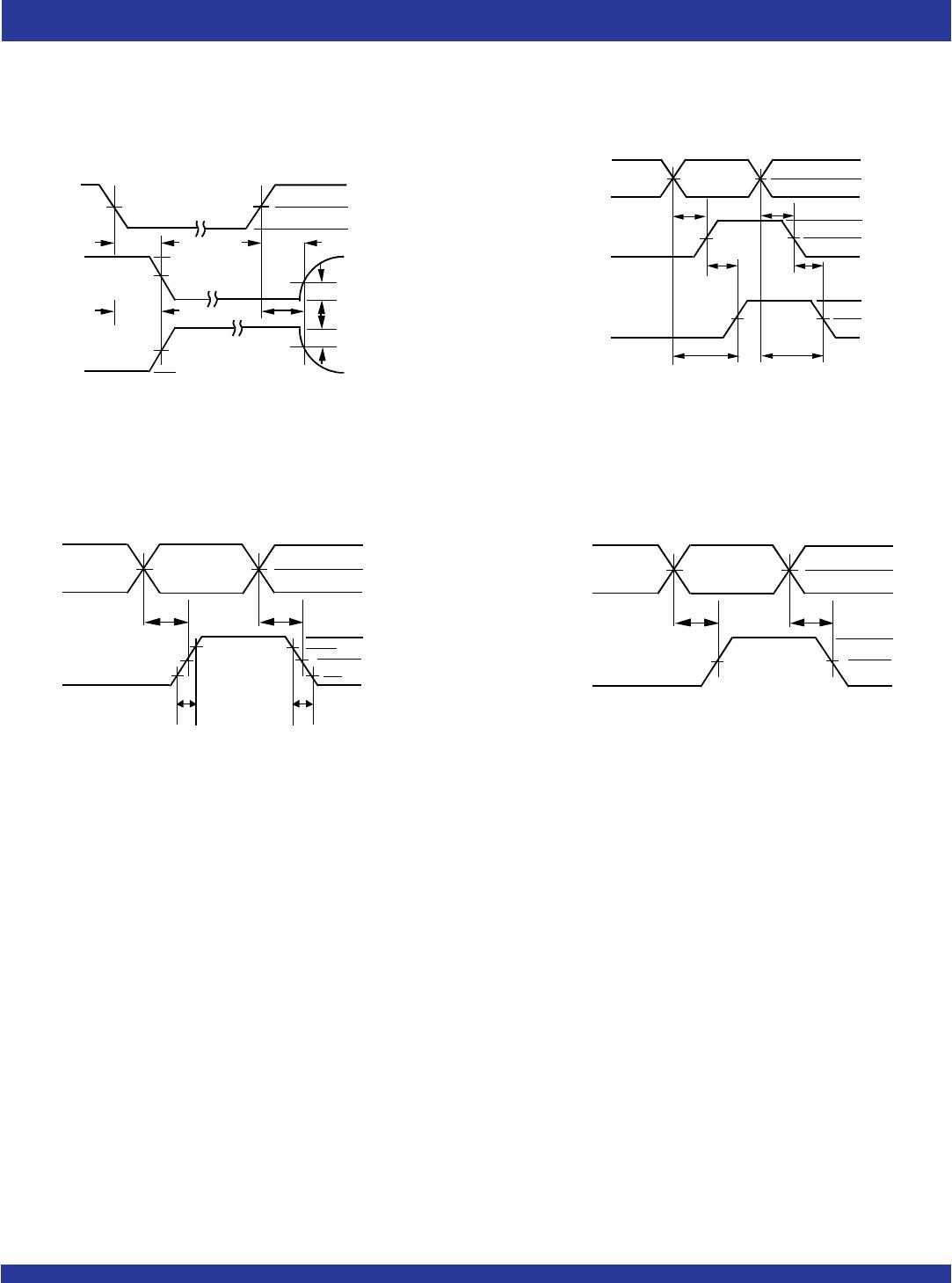
NOTES:
1. See test circuits and waveforms.
2. Minimum limits are guaranteed but not tested on Propagation Delays.
3. tPLH, tPHL, tSK(P), and tSK(O) are production tested. All other parameters guaranteed but not production tested.
4. Propagation delay range indicated by Min. and Max. limit is due to VCC, operating temperature and process parameters. These propagation delay limits do not imply skew.
5. Skew measured between all outputs under identical transitions and load conditions.
6. Skew measured is difference between propagation delay times tPHL and tPLH of same outputs under identical load conditions.
7. Part to part skew for all outputs given identical transitions and load conditions at identical VCC levels and temperature.
8. Airflow of 1m/s is recommended for frequencies above 133MHz.
9. This parameter is measured using f = 1MHz.
SWITCHING CHARACTERISTICS OVER OPERATING RANGE - 3805E
(3,4)
Symbol Parameter Conditions
(1,8)
Min.
(2)
Max. Unit
tPLH Propagation Delay CL = 15pF 0.5 2.5 ns
tPHL INA to OAn, INB to OBn f ≤ 166MHz
tR Output Rise Time (0.8V to 2V) — 1 ns
tF Output Fall Time (2V to 0.8V) — 1 ns
tSK(O) Same device output pin to pin skew
(5)
— 200 ps
tSK(P) Pulse skew
(6,9)
— 270 ps
tSK(PP) Part to part skew
(7)
— 550 ps
t
PZL Output Enable Time — 5.2 ns
tPZH OEA to OAn, OEB to OBn
tPLZ Output Disable Time — 5.2 ns
tPHZ OEA to OAn, OEB to OBn
fMAX Input Frequency — 166 MHz