IXYS Reserves the Right to Change Limits, Test Conditions, and Dimensions.
IXYK100N120B3
IXYX100N120B3
IXYS MOSFETs and IGBTs are covered 4,835,592 4,931,844 5,049,961 5,237,481 6,162,665 6,404,065 B1 6,683,344 6,727,585 7,005,734 B2 7,157,338B2
by one or more of the following U.S. patents: 4,860,072 5,017,508 5,063,307 5,381,025 6,259,123 B1 6,534,343 6,710,405 B2 6,759,692 7,063,975 B2
4,881,106 5,034,796 5,187,117 5,486,715 6,306,728 B1 6,583,505 6,710,463 6,771,478 B2 7,071,537
Notes:
1. Pulse test, t ≤ 300μs, duty cycle, d ≤ 2%.
2. Switching times & energy losses may increase for higher V
CE
(clamp), T
J
or R
G
.
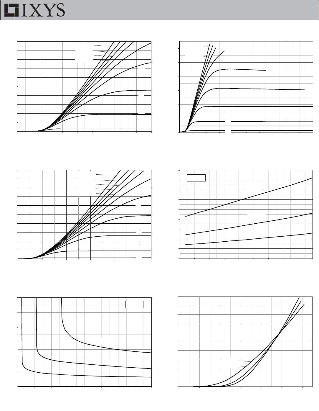
Symbol Test Conditions Characteristic Values
(T
J
= 25°C Unless Otherwise Specified) Min. Typ. Max.
g
fs
I
C
= 60A, V
CE
= 10V, Note 1 30 52 S
C
ie
s
6000 pF
C
oes
V
CE
= 25V, V
GE
= 0V, f = 1MHz 367 pF
C
res
127 pF
Q
g(on)
250 nC
Q
ge
I
C
= I
C110
, V
GE
= 15V, V
CE
= 0.5 • V
CES
42 nC
Q
gc
96 nC
t
d(on)
30 ns
t
ri
90 ns
E
on
7.7 mJ
t
d(off)
153 ns
t
fi
240 ns
E
of
f
7.1 11.5 mJ
t
d(on)
29 ns
t
ri
96 ns
E
on
11.4 mJ
t
d(off)
190 ns
t
fi
260 ns
E
off
10.1 mJ
R
thJC
0.13 °C/W
R
thCS
0.15 °C/W
Inductive load, T
J
= 25°C
I
C
= I
C110
, V
GE
= 15V
V
CE
= 0.5 • V
CES
, R
G
= 1Ω
Note 2
Inductive load, T
J
= 150°C
I
C
= I
C110
, V
GE
= 15V
V
CE
= 0.5 • V
CES
, R
G
= 1Ω
Note 2
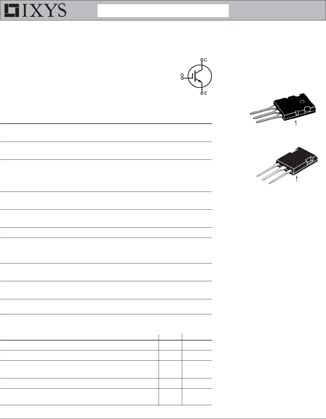
TO-264 Outline
Terminals: 1 = Gate
2,4 = Collector
3 = Emitter
Terminals: 1 - Gate
2 - Collector
3 - Emitter
PLUS247
TM
Outline
Dim. Millimeter Inches
Min. Max. Min. Max.
A 4.83 5.21 .190 .205
A
1
2.29 2.54 .090 .100
A
2
1.91 2.16 .075 .085
b 1.14 1.40 .045 .055
b
1
1.91 2.13 .075 .084
b
2
2.92 3.12 .115 .123
C 0.61 0.80 .024 .031
D 20.80 21.34 .819 .840
E 15.75 16.13 .620 .635
e 5.45 BSC .215 BSC
L 19.81 20.32 .780 .800
L1 3.81 4.32 .150 .170
Q 5.59 6.20 .220 0.244
R 4.32 4.83 .170 .190
PRELIMANARY TECHNICAL INFORMATION
The product presented herein is under development. The Technical Specifications offered are derived
from a subjective evaluation of the design, based upon prior knowledge and experience, and constitute a
"considered reflection" of the anticipated result. IXYS reserves the right to change limits, test
conditions, and dimensions without notice.